Semiconductor manufacturing method of die-pick-up from wafer

a manufacturing method and semiconductor technology, applied in the direction of adhesives, basic electric elements, electric devices, etc., can solve the problems of chip cracking under local stress, difficult peeling off of dicing tape, and inability to completely separate the die attach film, etc., to achieve rapid chip picking and reduce the cost of the device

Inactive Publication Date: 2006-07-27
RENESAS ELECTRONICS CORP
View PDF1 Cites 68 Cited by
  • Summary
  • Abstract
  • Description
  • Claims
  • Application Information

AI Technical Summary

Benefits of technology

[0089] The chips affixed to the dicing tape through the die attach film can be picked up rapidly without the occurrence of cracking or chipping.
[0090] It is possible to reduce the cost of the device for picking up the chips affixed to the dicing tape.

Problems solved by technology

However, in the case where a die attach film is interposed between the wafer and the dicing tape, the adjacent die attach film cannot be separated completely even if full-cut dicing is performed and hence the chips are difficult to peel off from the dicing tape.
However, if a chip is picked up in a stretched state of the dicing tape, the chip may be cracked under the imposition of a local stress thereon.
Particularly, as a recent tendency, chips formed thin to a thickness of several ten μm or so are often used to promote a high-density semiconductor packaging, thus giving rise to the problem that a crack is apt to occur at the time of pickup.

Method used


Image

  • Semiconductor manufacturing method of die-pick-up from wafer
  • Semiconductor manufacturing method of die-pick-up from wafer
  • Semiconductor manufacturing method of die-pick-up from wafer

Examples


first embodiment

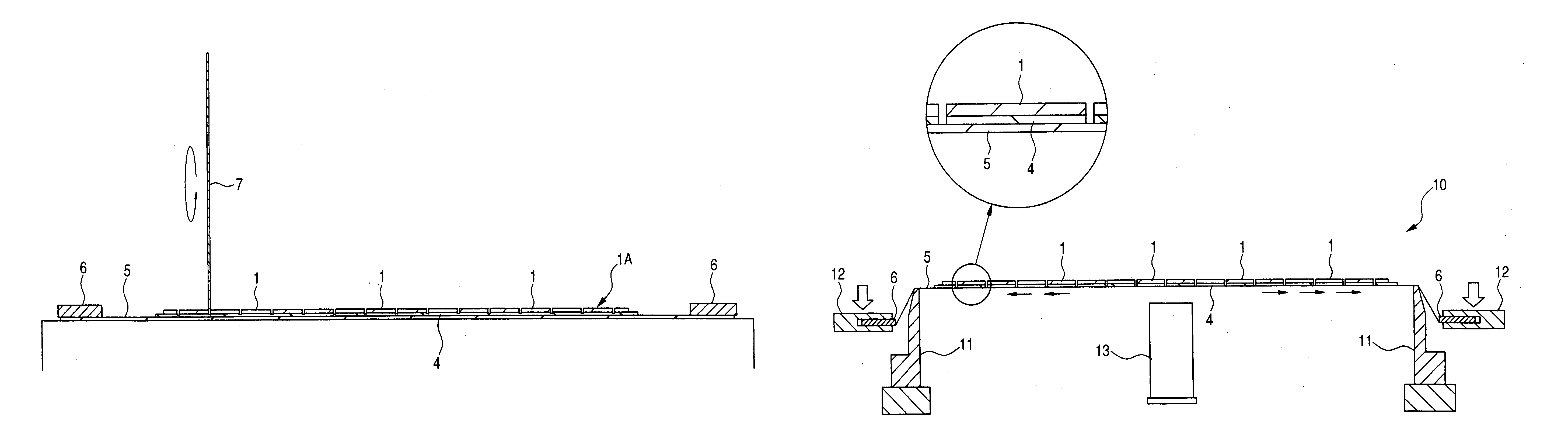
[0129] A manufacturing method of a semiconductor device according to a first embodiment of the present invention will be described below step by step with reference to FIGS. 1 to 21.

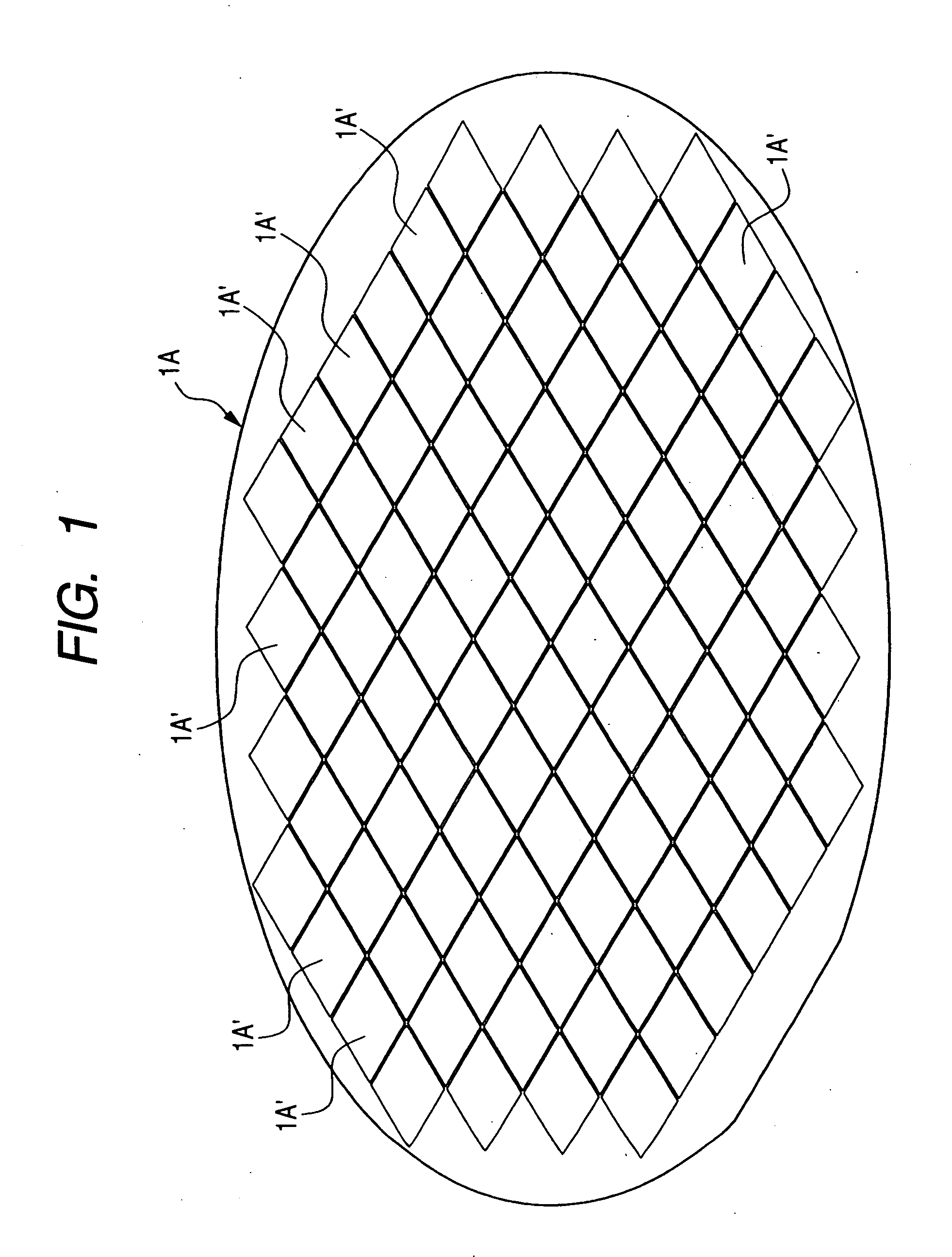
[0130] First, there is provided such a wafer 1A of a single crystal silicon as shown in FIG. 1. A main surface of the wafer 1A is partitioned into plural chip regions 1A′ and an integrated circuit is formed on each chip region 1A′ by a known semiconductor manufacturing process.

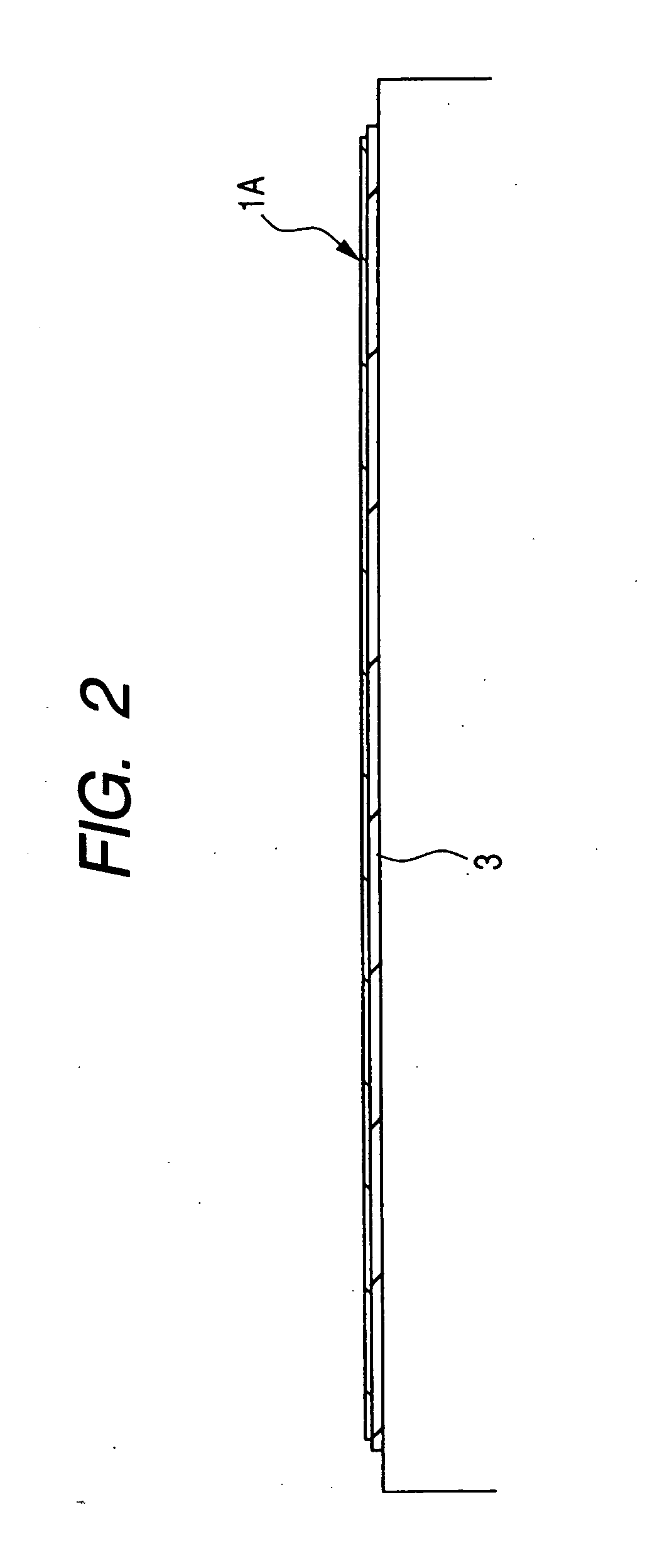
[0131] Next, as shown in FIG. 2, a back grinding tape 3 for protection of the integrated circuit is affixed to the main surface (the lower surface side in the figure) of the wafer 1A. In this state, grinding is performed for a back surface (the upper surface side in the figure) of the wafer 1A by means of a grinder and thereafter a damaged layer resulting from the grinding is removed by such a method as wet etching, dry polishing or plasma etching, thereby thinning the wafer 1A to a thickness of not larger than 100 μm, e.g., 30 t...

second embodiment

[0161] In the previous first embodiment a description was directed mainly to the die bonding method for chips 1 with use of the die attach film 4, while in this second embodiment a description will be given about a die bonding method for chips 1 with use of paste.

[0162]FIG. 29 is a perspective view showing an appearance of a dispenser used in this second embodiment, FIG. 30 is a plan view of a sealing disc as a mechanical part of the dispenser, and FIG. 31 is a sectional view taken along line A-A in FIG. 30.

[0163] In a dispenser 50 used in this second embodiment, only the structure of a sealing disc 51 is different from the dispenser 60 shown in the foregoing FIGS. 34 to 36. Therefore, other mechanical parts will be referred to using the same reference numerals as those of the mechanical parts of the dispenser 60.

[0164] As shown in FIGS. 30 and 31, a suction hole 52 which is put in communication with a suction port 64 and a discharge hole 53 which is put in communication with a d...


PUM


Abstract

A manufacturing method of a semiconductor device comprising the steps of: affixing a die attach film and a dicing film to a back surface of a semiconductor wafer: thereafter dicing the semiconductor wafer and the die attach film to divide the semiconductor wafer into a plurality of semiconductor chips: thereafter pulling the dicing film from the center toward the outer periphery of the dicing film with a first tensile force to cut the die attach film chip by chip; and thereafter picking up the semiconductor chips together with the die attach film while pulling the dicing film from the center toward the outer periphery of the dicing film with a second tensile force smaller than the first tensile force.

Description

CROSS-REFERENCE TO RELATED APPLICATION [0001] The present application claims priority from Japanese patent application No. 2005-013690 filed on Jan. 21, 2005, the content of which is hereby incorporated by reference into this application. BACKGROUND OF THE INVENTION [0002] The present invention relates to a semiconductor device manufacturing technique and more particularly to a technique applicable effectively to the step of dividing a semiconductor wafer affixed to a dicing film into plural semiconductor chips and thereafter separating the semiconductor chips from the dicing film and the step of mounting each of the separated semiconductor chips onto a mounting base through a die bonding paste. [0003] As steps included in a process of mounting a semiconductor chip (hereinafter referred to simply as “chip”) onto a mounting base such as a wiring substrate or a lead frame to assemble a semiconductor package there are a pickup step of separating a chip from a semiconductor wafer (simpl...

Claims


Application Information

Patent Timeline
Patent Type & Authority Applications(United States)
IPC IPC(8): H01L21/78H01L21/301H01L21/46
CPCH01L21/67132Y10T156/1132Y10T156/1092Y10T156/1077Y10T156/1089Y10T156/1179Y10T156/1983
Inventor MAKI, HIROSHISEIKI, KAZUHIROWADA, EIJI
Owner RENESAS ELECTRONICS CORP
Why Eureka
Try Eureka