Semiconductor device and method of manufacturing thereof

a semiconductor device and semiconductor technology, applied in semiconductor devices, semiconductor/solid-state device details, electrical apparatus, etc., can solve the problems of difficult high-speed transmission, high wiring density on mounting substrates, and long wiring length between chips, so as to shorten the length reduce the cost of the semiconductor device, and improve the effect of transmission speed

Inactive Publication Date: 2006-08-03
RENESAS ELECTRONICS CORP
View PDF1 Cites 91 Cited by
  • Summary
  • Abstract
  • Description
  • Claims
  • Application Information

AI Technical Summary

Benefits of technology

[0025] (4) The connection between the upper and lower chips may be without through a mounting substrate, different from a method using wire-bonding, and accordingly, the mounting substrate may be formed with only a wiring layer which is connected from a lowermost semiconductor chip to external electrodes, thereby it is possible to constitute a structure of two or four layer substrates. Accordingly, in comparison with currently used substrates which are formed of multilayered build-up substrates, it is possible to aim at thinning a semiconductor device and lowering the costs thereof; and
[0026] (5) In the case of lamination of different kinds of semiconductor chips, an interposer chip interposed, for example, between upper and lower chips in lamination may be formed even on the rear surface side with a rewiring layer, simultaneously, within a process range in which the piercing electrodes are formed. Thus, a two layer wiring layout may be substantially made, and accordingly, an inexpensive chip configuration having only one aluminum surface wiring layer may be normally used as the interposer chip. That is, in comparison with a connecting process, as disclosed in the prior art documents, with the use of piercing electrodes, a configuration and a process which are extremely inexpensive with a short TAT may be used, and an unique connection structure with a high degree of reliability may be materialized due to calking with the use of deformation of the metal bumps caused by plastic flow, thereby it is possible to provide a configuration of three-dimensional inter-chip connection which is highly practical.

Problems solved by technology

Thus, there have been raised a problem of a long wiring length between the chips, and a problem of an extremely high wiring density on the mounting substrate.
Thus, an inductance between chips is increased, and accordingly, high speed transmission becomes difficult.
Further, the high wiring density on the mounting substrate causes a lower yield, resulting in an increase in the costs of the mounting substrate.
Thus, there may be raised not only such a problem that an inductance between the chips increases so as to cause difficulty in high speed transmission and but also such a problem that the higher density of the mounting substrate deteriorates the yield so as to increase the substrate costs.
However, due to a laminated structure in which individual packages are laminated one upon another, there have been raised such problems that a wiring length becomes longer between chips, and that the freedom in the case of lamination of different kinds of chips having different sizes has to be limited.
However, there will be caused in future such a problem that the wiring length causes a bottle neck problem in view of high speed transmission and miniaturization and thinning of the package in view of ensuring its bonding area.
Accordingly, should the piercing electrodes to be used for connection between chips by a mounting process, be formed also in the devise manufacturing process, there would be caused problems of lowering a yield and a TAT as to the manufacture of devices.
Further, as disclosed in JP-A-2000-260934, in a method in which bump electrodes are formed in through holes in chips through plating growth, there would be raised a problem of taking a relatively long time for the plating growth (several hours) and a problem of incurring technical difficulty in uniform plating growth including through-holes having a high aspect ratio.
Further, different from a method using wire bonding, semiconductor chips which are laminated on the upper stage side are not directly connected to external electrodes through the intermediary of mounting substrates.
Further, with a multi-stage lamination structure of the same kind of chips, there would be caused a problem of chip select for the upper stage semiconductor chip.

Method used


Image

  • Semiconductor device and method of manufacturing thereof
  • Semiconductor device and method of manufacturing thereof
  • Semiconductor device and method of manufacturing thereof

Examples


embodiment 1

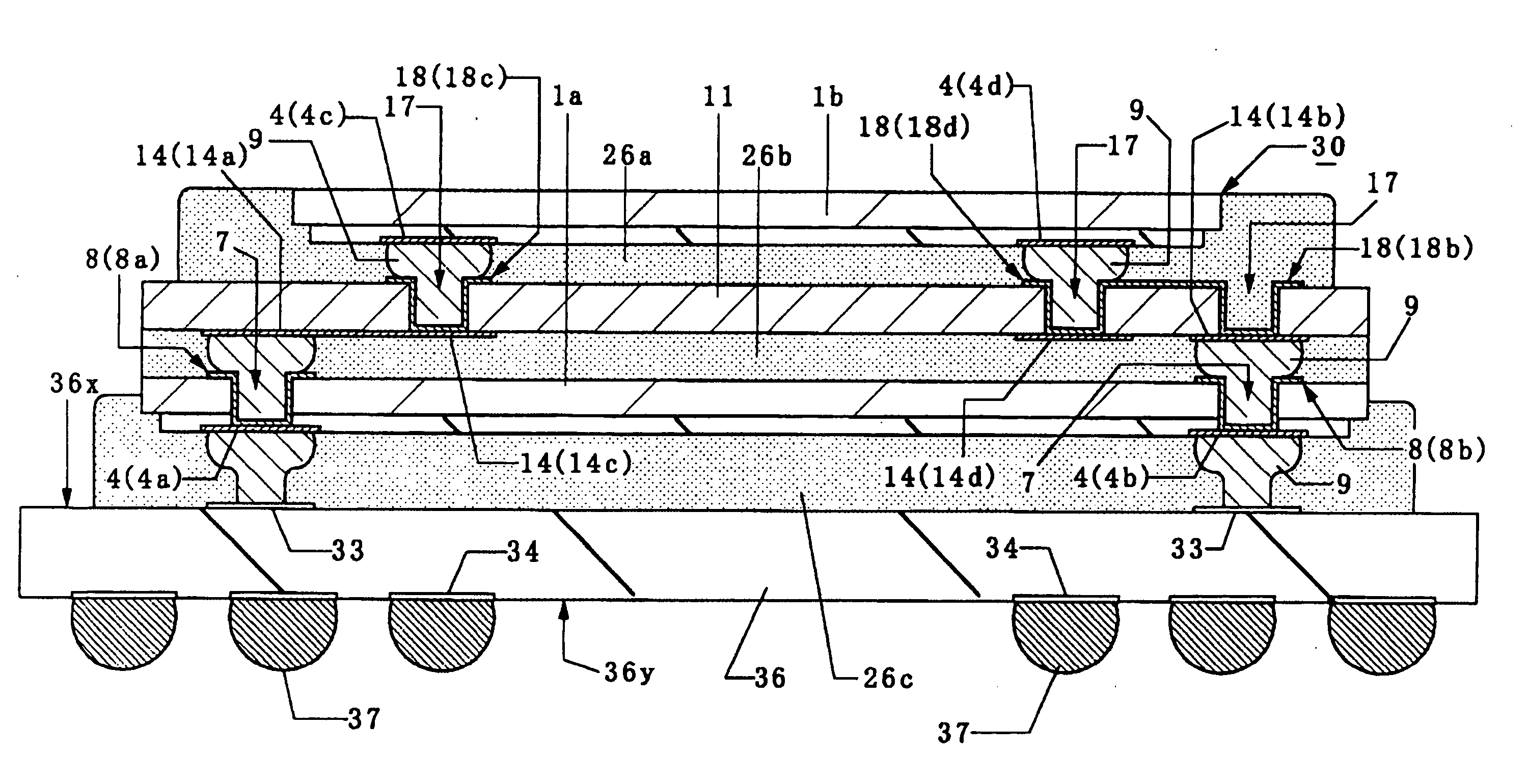
[0076] In the embodiment 1, a semiconductor device having a lamination in which different kinds of semiconductor chips are three-dimensionally laminated one upon another, an interposer chip (an intermediate wiring substrate) being interposed therebetween.

[0077] FIGS. 1 to 17b are views for explaining the semiconductor device in the embodiment 1 of the present invention, that is,

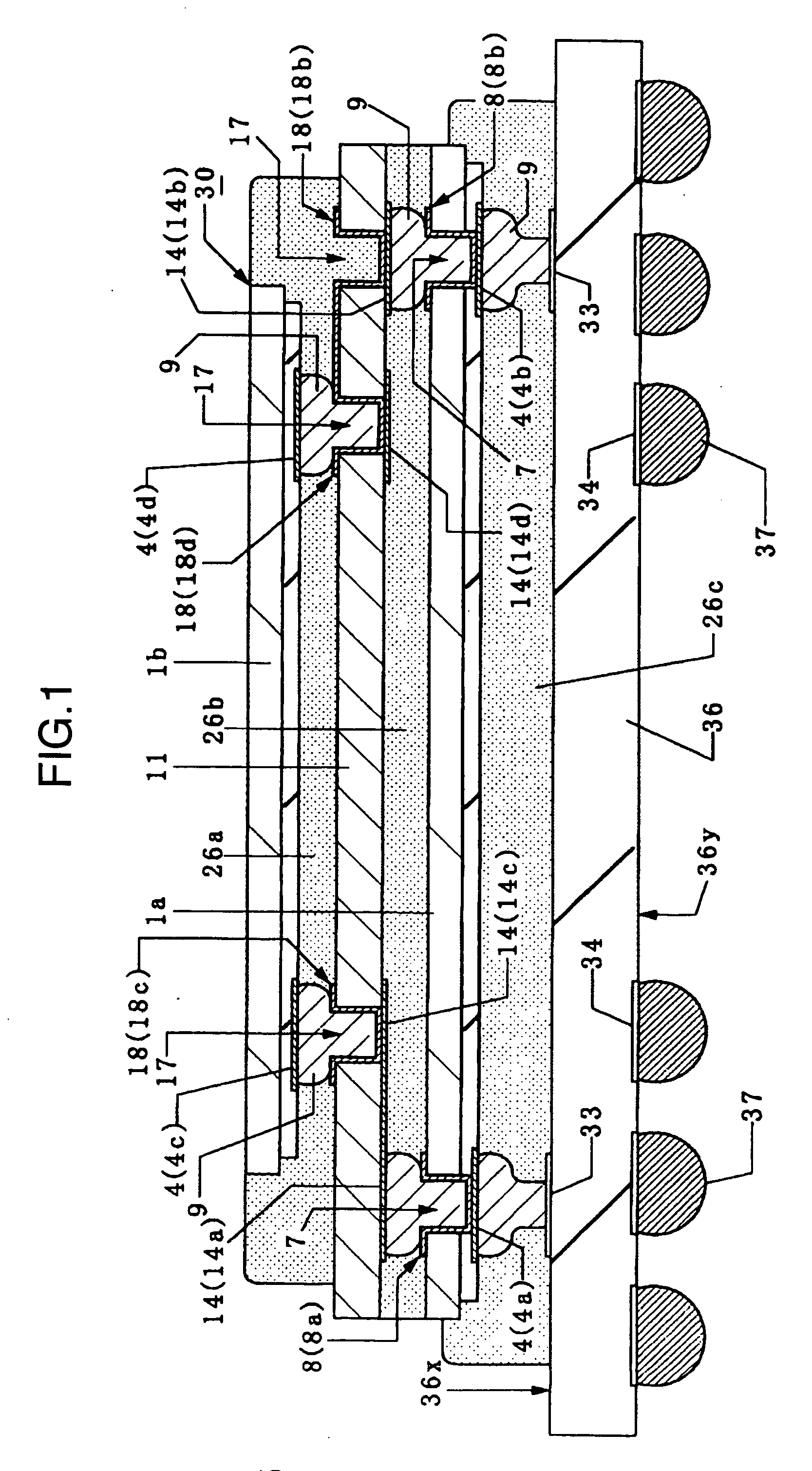
[0078]FIG. 1 is a schematic view illustrating the configuration of the semiconductor device;

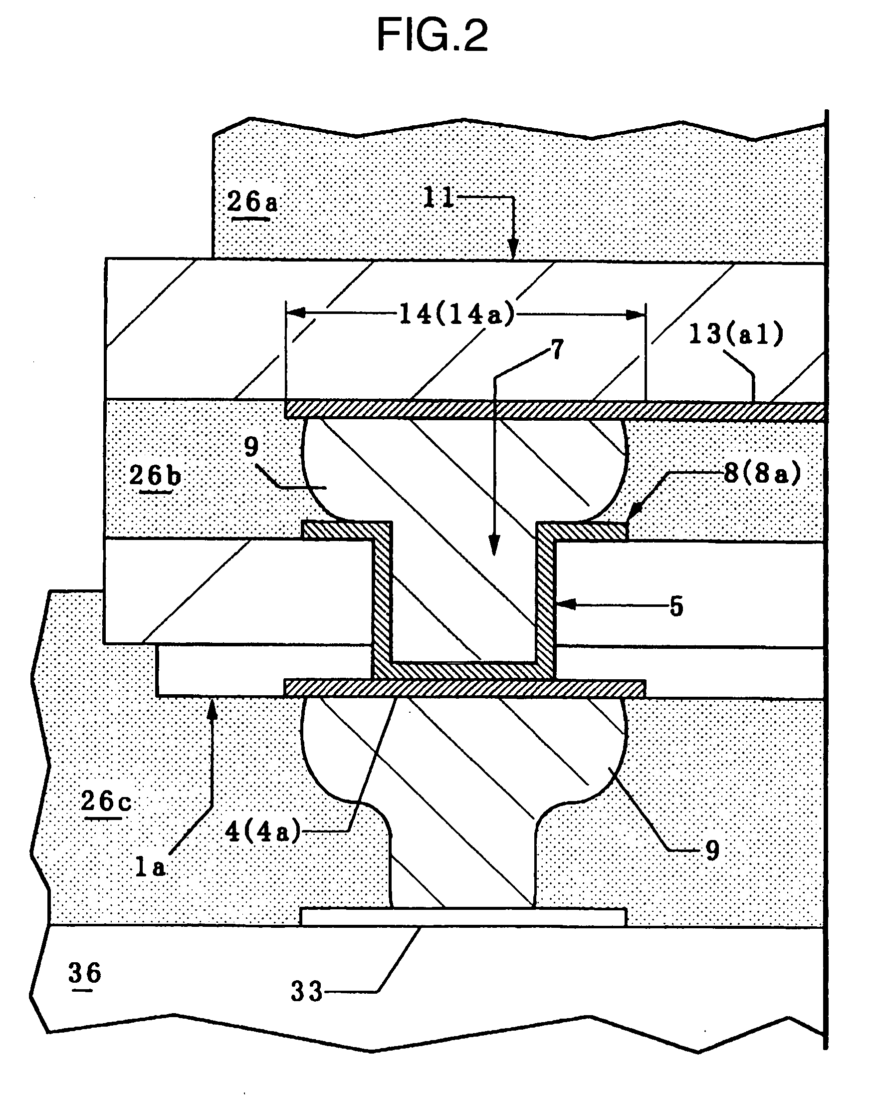
[0079]FIG. 2 is an enlarged schematic sectional view illustrating a part shown in FIG. 1;

[0080]FIG. 3a is a schematic sectional view illustrating an entire configuration of a semiconductor chip located at the lowermost stage in a chip lamination shown in FIG. 1:

[0081]FIG. 3b is an enlarged schematic sectional view illustrating a part in FIG. 3a;

[0082]FIG. 4a is a schematic sectional view illustrating an entire configuration of a semiconductor chip located at the uppermost stage in the chip lamination shown in FIG...

embodiment 2

[0202] FIGS. 25 to 26c show a semiconductor device in an embodiment 2 of the present invention, in which FIG. 25 is a schematic sectional view illustrating a configuration of the semiconductor device, FIG. 26a is a schematic sectional view illustrating a semiconductor chip located at the uppermost stage of a chip lamination, FIG. 26b is a schematic sectional view illustrating an interposer chip and FIG. 26c is a schematic sectional view illustrating a semiconductor chip located at the lowermost stage.

[0203] The semiconductor device in this embodiment 2 has the same configuration as that of the embodiment 1, except that the chip lamination has a different structure. As shown in FIG. 25, in the chip lamination 30a in this embodiment 2, a semiconductor chip 1d is laminated on a semiconductor chip 1a through the intermediary of an interposer chip 11a, the semiconductor chip 1d having an external size which is larger than that of the semiconductor chip 1c.

[0204] The upper stage semicon...

embodiment 4

[0218]FIG. 28 is a schematic sectional view illustrating a configuration of a semiconductor device in an embodiment 4.

[0219] Explanation has been made of the three-dimensional lamination of different kinds of upper and lower semiconductor chips between which the interposer chip 11 is interposed in order to materialize operative three-dimensional connection between the upper and lower semiconductor chips in the embodiment 1. However, in this embodiment 4, concave electrodes (8a, 8b) are formed at electrode positions (electrode pads 4a, 4b) on the rear surface 1y side of a lower stage semiconductor chip 1e, at which connection to an upper stage semiconductor chip is required, and simultaneously, a rewiring layer connected thereto and concave electrodes (8a, 8d) connected to the upper stage semiconductor chip 1b are formed. Thus, the upper stage semiconductor chip 1b is electrically connected to the lower stage semiconductor chip 1e, direct thereto.

[0220] Thus, there may be obtained ...


PUM


Abstract

A connection method for materializing a high-performance semiconductor system which is small-sized and high dense, is capable to three-dimensionally connecting a plurality of different kinds of semiconductor chips through piercing electrodes with shortest wiring lengths. The connection method enables high-speed operation with low noise, so as to obtain reliable and excellent connection in a short TAT at low costs. In a three-dimensional chip lamination composed of different kinds of semiconductor chips laminated one upon another with an interpose chip being interposed therebetween for connecting the upper and lower semiconductor chips, the semiconductor chips and the interposer chips are polished by grinding or the like at their rear surfaces so as to have thin thickness, holes are formed at rear surface positions corresponding to external electrode parts on the device side (front surface side) so that the holes extend to front surface electrodes, by dry etching or the like, and metal plating films are applied to the side walls of the holes and rear surface side, metal bumps of another semiconductor chip laminated at an upper stage being press-fitted into the holes applied with the metal plating films through deformation and being geometrically calked in the through holes formed in the semiconductor chip so as to electrically connected thereto.

Description

BACKGROUND OF THE INVENTION [0001] The present invention relates to a semiconductor device having a plurality of semiconductor chips which are three-dimensionally laminated one upon another. [0002] These years, there has been spotlighted to a technology of system packages in which several semiconductor chips incorporated therein integrated circuits are densely packaged, and which have a high performance, and accordingly, several firms have proposed several various packaging configurations. In particular, there have been prosperously developed laminated packages in which several semiconductor chips are three-dimensionally packaged so as to be allow the packages to be comparatively small-sized. [0003] Since wire-bonding is in general utilized for electrical connection between a substrate and a semiconductor chip mounted thereon, it is required that the sizes of the semiconductor chips to be laminated one upon another are set, the higher the laminated stage, the smaller the size of the...

Claims


Application Information

Patent Timeline
Patent Type & Authority Applications(United States)
IPC IPC(8): H01L23/52
CPCH01L23/481H01L24/72H01L24/97H01L25/0657H01L2224/16145H01L2224/16237H01L2224/97H01L2225/06513H01L2225/06527H01L2225/06541H01L2225/06572H01L2225/06593H01L2924/01005H01L2924/01013H01L2924/01029H01L2924/01078H01L2924/01079H01L2924/14H01L2924/15311H01L2924/18161H01L2924/19041H01L2924/30105H01L2924/30107H01L2924/3011H01L2224/81H01L2924/01006H01L2924/01024H01L2924/01033H01L2924/12041H01L24/05H01L24/13H01L24/16H01L24/81H01L2224/81191H01L2224/81385H01L2224/81898
Inventor TANAKA, NAOTAKAYOSHIMURA, YASUHIRONAITO, TAKAHIROAKAZAWA, TAKASHI
Owner RENESAS ELECTRONICS CORP
Why Eureka
Try Eureka