Clamp for use in processing semiconductor workpieces

a technology for semiconductor workpieces and clamps, which is applied in semiconductor/solid-state device manufacturing, basic electric elements, electric apparatus, etc., can solve the problems of insufficient clamping force of wafer devices, inability to apply aluminum oxynitride for electrostatic clamps, and damage to charging current devices on the wafer. , to achieve the effect of prolonging the lifetim

Active Publication Date: 2006-08-03
VARIAN SEMICON EQUIP ASSOC INC
View PDF13 Cites 22 Cited by
  • Summary
  • Abstract
  • Description
  • Claims
  • Application Information

AI Technical Summary

Benefits of technology

[0008] It is the general object of this present invention to provide improved methods and apparatus for clamping of a workpiece to a support surface.
[0009] According to a first aspect of the invention, an apparatus comprises a support base, an insulator layer disposed on the support base, an electrode layer disposed on the insulator layer, and a clamping layer comprising aluminum oxynitride disposed on the electrode layer wherein the workpiece is clamped to the surface of the clamping layer. The apparatus provides a higher clamping force for the workpiece while reducing gas leakage and particle levels in addition to maintaining a declamping time suitable for high throughput processing.
[0010] According to another aspect of the invention, an apparatus comprises a support base, an insulator layer disposed on the support base, an electrode layer disposed on the insulator layer, and a clamping layer comprising a dielectric layer and a resilient material layer disposed on the electrode layer wherein the workpiece is clamped to the surface of the clamping layer. The apparatus and configurations of the dielectric and resilient layers further reduce backside particle generation while providing a high clamping force for the workpiece.

Problems solved by technology

Aluminum oxynitride was not believed to be applicable for electrostatic clamps due the difficulty in processing aluminum oxynitride powders and manufacturability of the very thin dielectric layer, in addition to unknown technical performance characteristics.
Problems associated with electrostatic clamps disclosed in U.S. Pat. No. 6,388,861 include insufficient wafer clamping force, charging current damage to devices on the wafer, difficulty in making electrical contact to the semiconductor wafer, wafer declamp time, and inadequate transfer of heat from a semiconductor wafer work piece.

Method used


Image

  • Clamp for use in processing semiconductor workpieces
  • Clamp for use in processing semiconductor workpieces
  • Clamp for use in processing semiconductor workpieces

Examples


Embodiment Construction

[0035] According to the present invention, these objects and advantages are achieved in the apparatus for electrostatic clamping of workpieces as indicated in the following figures.

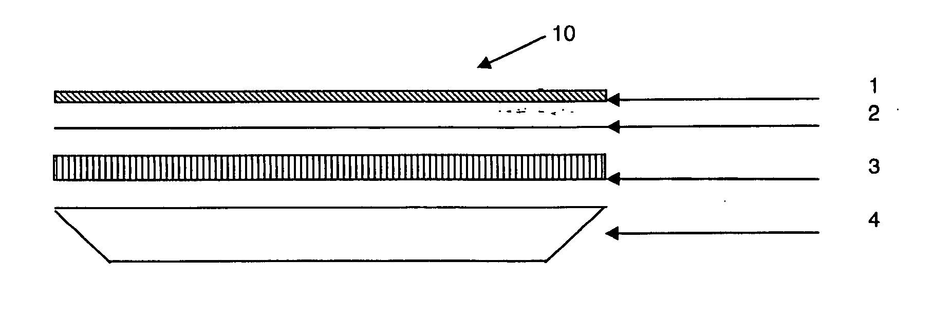
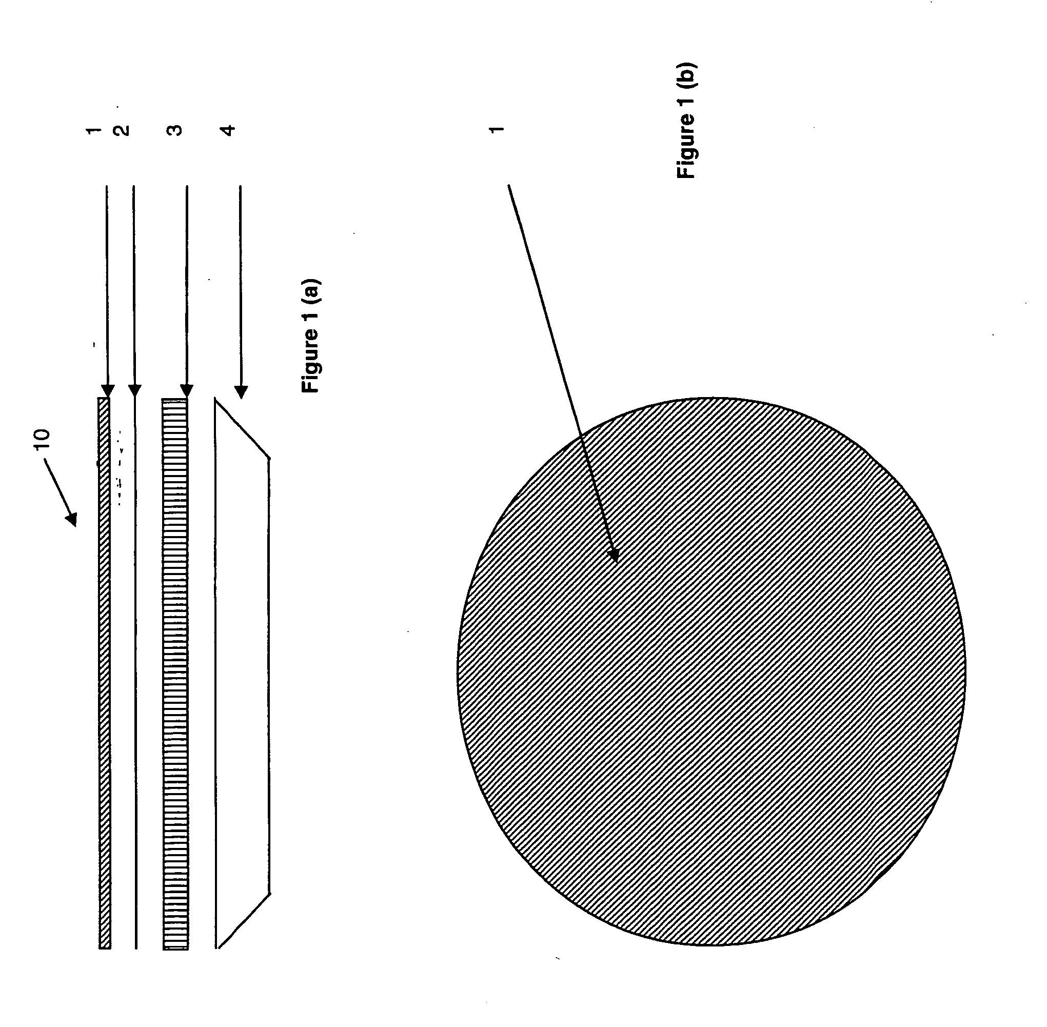
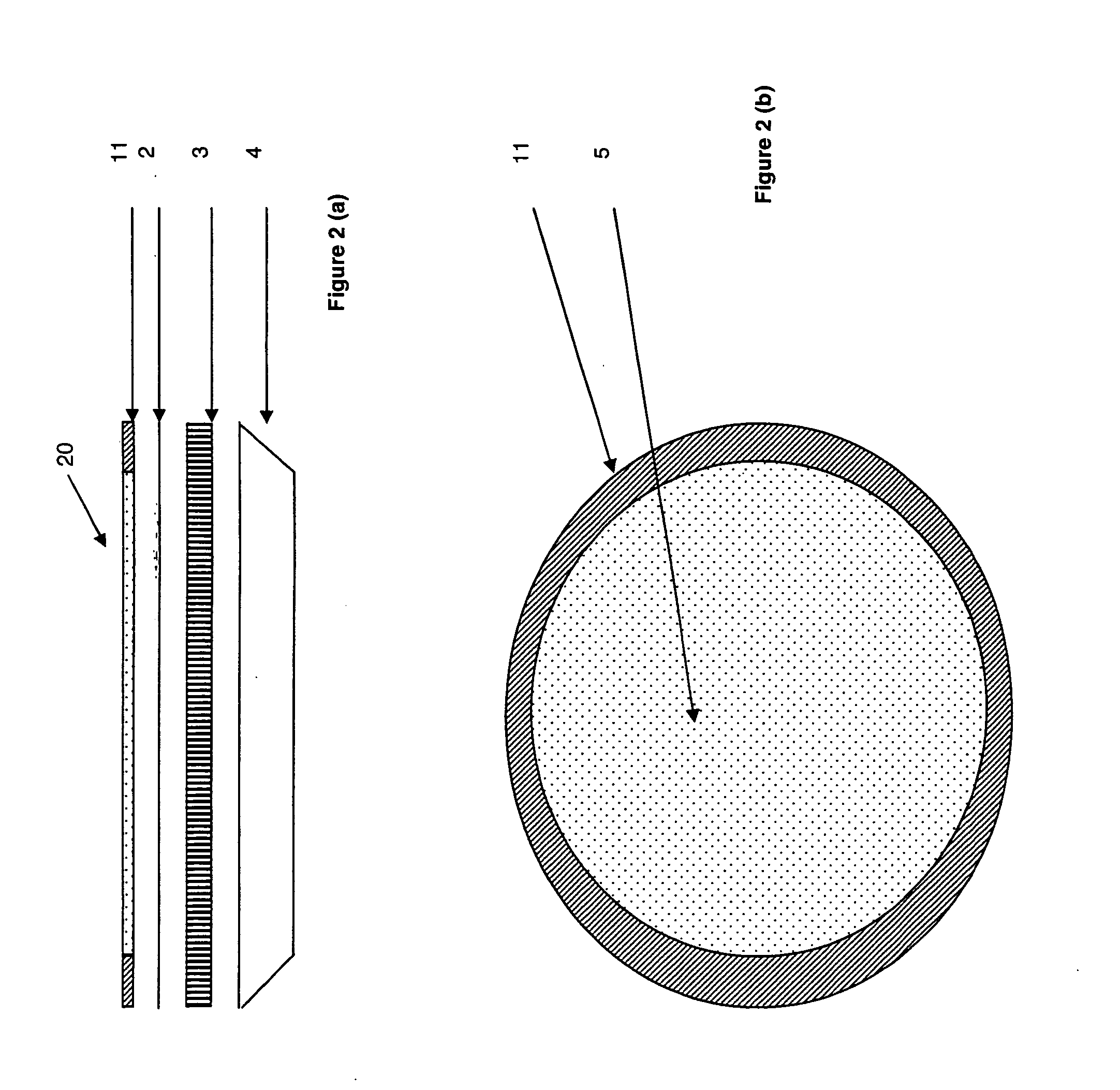
[0036] One embodiment of a clamp 10 is shown in FIGS. 1(a) and 1(b) wherein the dielectric layer 1 may be comprised of aluminum oxynitride and the insulator layer 3 may be comprised of alumina. The electrode 2 may be made of metal and a support base 4 of aluminum. Cooling gas is distributed via conventional cooling gas holes in the electrostatic clamp surface. A workpiece may be electrostatically or mechanically clamped to the clamping surface using known electrostatic or mechanical clamping techniques. An electrostatic clamp 10 of such a design has been fabricated and tested in an ion implanter. Test results indicate that the aluminum oxynitride can yield higher clamping force, lower gas leakage, lower particle levels and longer lifetime due to the material's durability, along with a declamping time com...


PUM


Abstract

An apparatus is provided to improve clamping of a work piece to a support surface. The apparatus includes a support base, an insulator layer disposed on the support base, an electrode layer disposed on the insulator layer, and a clamping layer comprising aluminum oxynitride disposed on the electrode layer wherein the workpiece is clamped to the surface of the clamping layer. The apparatus provides a higher clamping force for the workpiece while reducing gas leakage and particle levels in addition to maintaining a declamping time suitable for high throughput processing. The apparatus may further provide a raised surface geometry or embossments on the dielectric or a dielectric comprising an outer ring a center cavity for reducing particle contamination to the backside of the workpiece. Also, a thin wall sleeve may be provided between the base and the insulator and alternating current may be applied to opposite ones of interdigitated electrode pairs to reduce particle contamination and improve the implantation uniformity.

Description

RELATED APPLICATIONS [0001] This application is a continuation-in-part of U.S. Ser. No. 11 / 101,832 filed Apr. 8, 2005, entitled “Clamp For Use In Processing Semiconductor Workpieces,” the disclosure of which is hereby incorporated by reference. [0002] This application claims priority under 35 U.S.C. § 119(e) to U.S. Provisional Patent Application Ser. No. 60 / 560,912, filed Apr. 9, 2004, entitled “Electrostatic Clamp For Use In Processing Semiconductor Workpieces,” the disclosure of which is hereby incorporated by reference. BACKGROUND [0003] In the fabrication of integrated circuits, a number of well-established processes involve the application of ion beams to semiconductor wafers in vacuum. These processes include, for example, ion implantation, ion beam milling, and reactive ion etching. In each instance, an ion beam is generated in a source and is directed with varying degrees of acceleration toward a target wafer. Ion implantation has become a standard technique for introducing...

Claims


Application Information

Patent Timeline
Patent Type & Authority Applications(United States)
IPC IPC(8): H01T23/00
CPCH01L21/6831H01L21/6875H01L21/68757
Inventor MUKA, RICHARDMURPHY, PAULSUURONEN, DAVID E.
Owner VARIAN SEMICON EQUIP ASSOC INC
Why Eureka
Try Eureka