Light emitting device and method of making the same

a light emitting device and wavelength conversion technology, which is applied in the direction of solid-state devices, semiconductor devices for light sources, lighting and heating apparatus, etc., can solve the problems of difficult to secure long-term reliability, low brightness of light emitting devices, and complicated manufacturing processes, so as to enhance sealing properties and reliability, the effect of suppressing the deterioration caused by light emitted from the light emitting element and stable brightness

Inactive Publication Date: 2006-08-03
TOYODA GOSEI CO LTD
View PDF9 Cites 143 Cited by
  • Summary
  • Abstract
  • Description
  • Claims
  • Application Information

AI Technical Summary

Benefits of technology

[0076] According to the invention, since the light emitting element and the substrate both made of the inorganic material are sealed with the inorganic sealing material, the sealing property and reliability can be enhanced. Further, deterioration caused by light emitted from the light emitting element can be suppressed, and a stable brightness can be kept without unevenness in emission color ov

Problems solved by technology

However, the semiconductor light emitting device in JP-A-2004-221619 has the following problems.
(1) It is difficult to secure its long-term reliability since the resin sealing portion and the phosphor cover deteriorate due to the light emitted from the GaN-based semiconductor light emitting element.
Further, the brightness of the light emitting device lowers due to the deterioration.
Therefore, the manufacturing process will be complicated and the manufacturing cost will increase.
Therefore, the light extraction efficiency may lower significantly.
However, the light emitting device in JP-A-11-177129

Method used


Image

  • Light emitting device and method of making the same
  • Light emitting device and method of making the same
  • Light emitting device and method of making the same

Examples


first embodiment

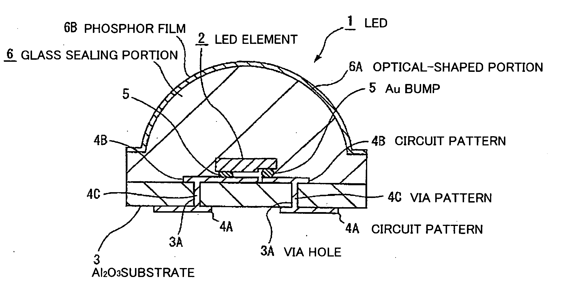
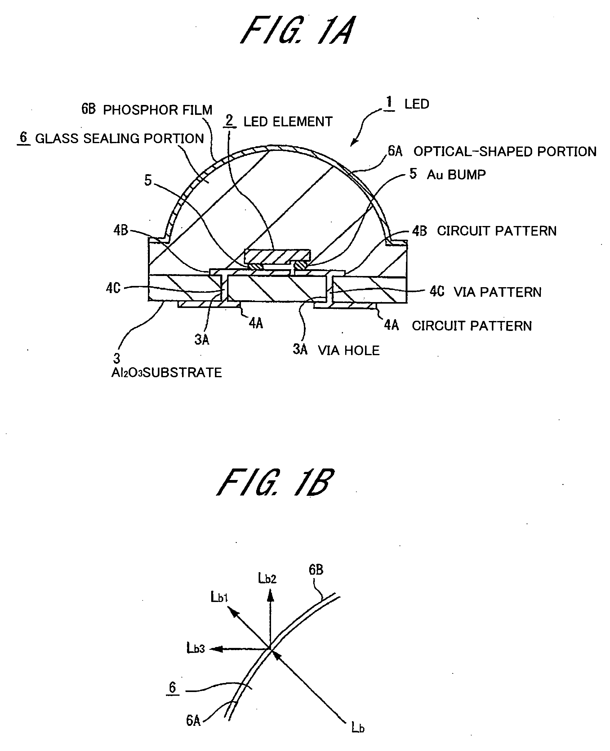
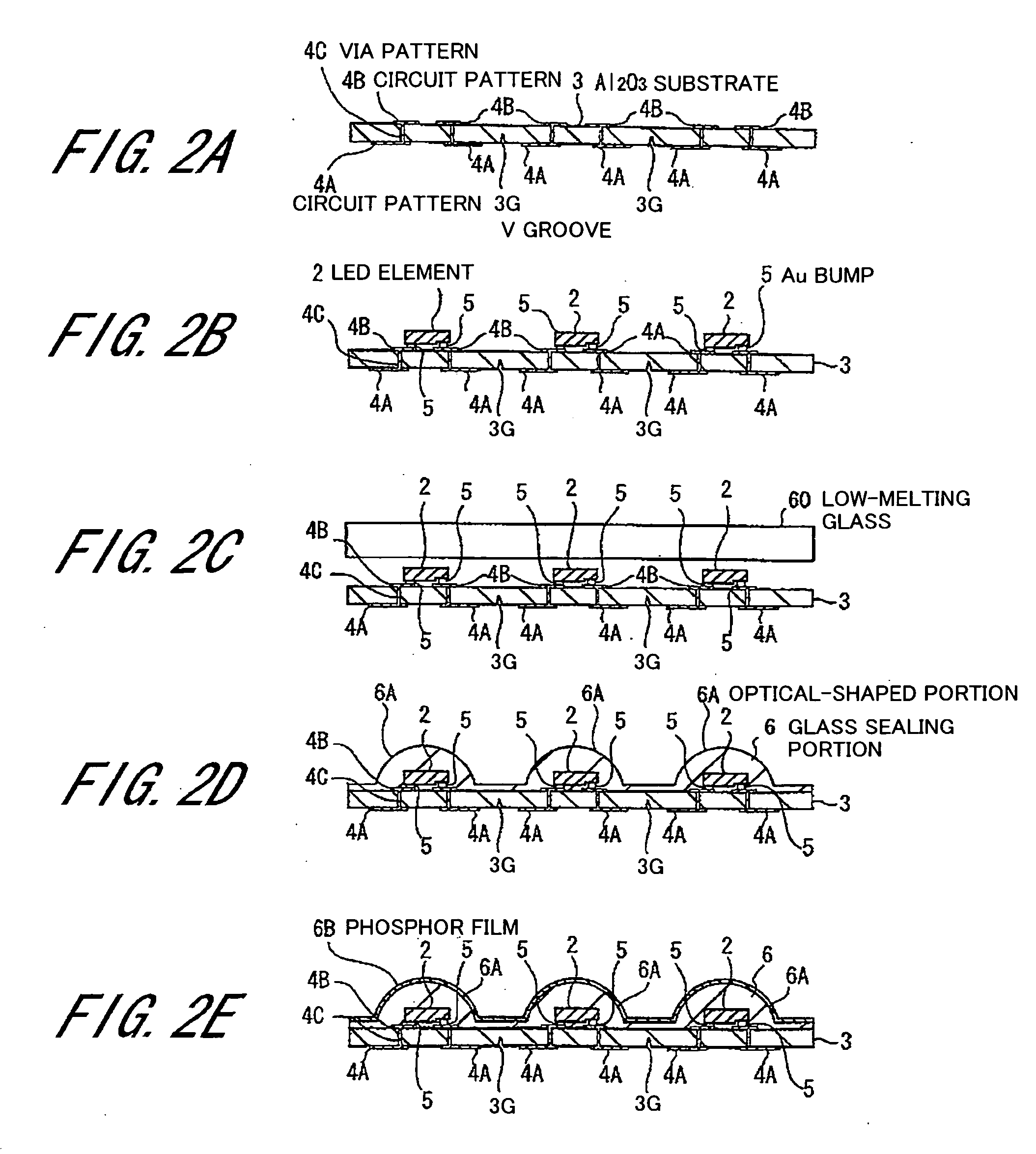
[0097]FIG. 1A is a cross sectional view showing a light emitting device in the first preferred embodiment according to the invention. FIG. 1B is a schematic diagram illustrating light radiation on the surface of a glass sealing portion.

Components of the Device

[0098] As shown in FIG. 1A, the LED 1 comprises: a flip-chip type LED element 2; an Al2O3 substrate 3, as an inorganic material substrate, provided with circuit patterns 4A, 4B, and via holes 3A; an Au bump 5 to electrically connect between the circuit pattern 4B and an electrode of the LED element 2; and a glass sealing portion 6 that is made of an inorganic sealing material to seal the Al2O3 substrate 3 and the LED element 2 and is provided with an optical-shaped portion 6A formed semispherical.

(Details of the Components)

[0099] The LED element 2 comprises, sequentially grown on an underlying sapphire substrate, an AlN buffer layer and a GaN-based semiconductor layer including an n-GaN layer, a light-emitting layer, and ...

second embodiment

[0128]FIG. 3 is a cross sectional view showing a light emitting device in the second preferred embodiment according to the invention. Hereinafter, like components are indicated by the same numerals used in the first embodiment.

(Components of the Device)

[0129] The LED 1 of the second embodiment is different from that of the first embodiment in that a phosphor-containing glass layer 6C is used in place of the phosphor film 6B of the first embodiment.

(Details of the Components)

[0130] The phosphor-containing glass layer 6C is made of a mixture material (with a melting point of about 300° C.) that a phosphor particle with an average outside diameter of 10 μm is mixed with a fluoride low-melting glass particle with an average outside diameter of 10 μm. The phosphor-containing glass layer 6C is formed integrally on the surface of the glass sealing portion 6 with the optical-shaped portion 6A by conducting the electrostatic coating of the mixture material while heating the glass seali...

third embodiment

[0133]FIG. 4 is a cross sectional view showing a light emitting device in the third preferred embodiment according to the invention.

(Components of the Device)

[0134] The LED 1 of the third embodiment is different from that of the first embodiment in that a dichroic mirror 6D is formed between the glass sealing portion 6 and the phosphor film 6B such that it prevents the re-entering of light radiated from the phosphor to the glass sealing portion 6.

(Details of the Components)

[0135] The dichroic mirror 6D is formed by laminating alternately TiO2 film and SiO2 film and severs to transmit light of less than 500 nm and to reflect light of more than 500 nm. Thus, the dichroic mirror 6D can transmit blue light of 470 nm emitted from the LED element 2 and reflect yellow light radiated from the phosphor of the phosphor film 6B to prevent the re-entering thereof to the glass sealing portion 6.

Effects of the Third Embodiment

[0136] In the third embodiment, the brightness can be enhanced ...


PUM


Abstract

A light emitting device having: a flip-mounting type light emitting element; a substrate on which the light emitting element is mounted, the substrate being of an inorganic material; a sealing portion to seal the light emitting element, the sealing portion being of an inorganic sealing material; an optical-shaped portion formed nearly semispherical, the optical-shaped portion being of the inorganic sealing material; and a phosphor portion formed covering the optical-shaped portion.

Description

[0001] The present application is based on Japanese patent application Nos. 2005-012810 and 2005-027484, the entire contents of which are incorporated herein by reference. BACKGROUND OF THE INVENTION [0002] 1. Field of the Invention [0003] This invention relates to a wavelength-conversion type light emitting device to wavelength-convert a light emitted from a light emitting element and, in particular, to a wavelength-conversion type light emitting device that is excellent in reliability, stable in brightness over a long term, and excellent in unevenness of emission color. [0004] Further, this invention relates to a light emitting device that the light emitting element is sealed with a glass sealing material and, in particular, to a light emitting device that is excellent in mass productivity, in sealing property and deterioration resistance under a high-temperature and high-humidity environment, and in evenness of emission color. [0005] Further, this invention relates to a method of...

Claims


Application Information

Patent Timeline
IPC IPC(8): F21S13/10
CPCF21K9/00H01L33/44H01L33/486H01L33/507H01L33/56H01L24/97H01L2924/1815H01L2224/48227H01L2224/48465H01L2224/48091H01L2924/12041H01L2224/16225H01L2924/00014H01L2924/00H01L2924/00011H01L2224/0401
Inventor SUEHIRO, YOSHINOBUYAMAGUCHI, SEIJI
Owner TOYODA GOSEI CO LTD
Why Eureka
Try Eureka