Supercharge Your Innovation With Domain-Expert AI Agents!

Internal data bus interconnection mechanism utilizing shared buffers supporting communication among multiple functional components of an integrated circuit chip

a technology of integrated circuit chips and buffers, applied in the direction of electric digital data processing, instruments, etc., can solve the problems of inability, cost, and complexity of modern computer systems, and achieve the effect of reducing the amount of buffer storage required and reducing the inherent delay of data passing

Inactive Publication Date: 2006-08-03
IBM CORP
View PDF23 Cites 15 Cited by
  • Summary
  • Abstract
  • Description
  • Claims
  • Application Information

AI Technical Summary

Benefits of technology

[0022] In the preferred embodiment, the integrated circuit chip is a bridge chip for coupling multiple data buses of a computer system. The functional modules within the chip are data bus interface modules for interfacing with the data buses, the data buses being external to the integrated circuit chip. The use of different functional modules coupled by the central interconnect enables the chip to support communications between buses of different types.
[0026] The use of a common central interconnect module with a shared buffer provides a low-overhead path for transferring data within the integrated circuit chip. The use of a shared buffer both reduces the amount of buffer storage required in the chip and reduces the inherent delay of data passing from one component to another. This architecture is readily adaptable to connect with functional components of different types, therefore supporting a variety of different specific ASIC designs.

Problems solved by technology

A modern computer system is an enormously complex machine, usually having many sub-parts or subsystems, each of which may be concurrently performing different functions in a cooperative, although partially autonomous, manner.
Each component of a digital computer system is itself a very complex instrument, having a design hierarchy which can mimic that of the system.
Unfortunately, this capability comes at a cost.
All of these operations take time.
Additionally, because the CPU is doing so many things at a time, it typically consumes a relatively large amount of power.
Such smaller, special-purpose digital logic circuits often consume less power than a typical CPU, and because they perform a more limited set of functions, often do so faster than a typical CPU.
It is simply more limited in the variety of functions it can perform.
Many ASICs are programmable to alter their functions within some design range, but in general they do not have the flexibility of a general-purpose CPU.
One of the challenge of using ASICs is the design effort involved.
Although the design of a single ASIC is no more difficult (and often less so) than that of a general-purpose processor, the number of different applications and consequent number of separate ASIC designs can involve a substantial burden in the design and development of a digital system using ASICs.
However, such special circuitry is likely to be different for each permutation of sender and receiver component module, depending on the requirements of the individual components.
On the other hand, it is possible to design a generic interface for communication among different functional components, but generic interfaces are likely to involve greater overhead and be less than optimal.
In some cases, it is possible to avoid this double buffering by taking advantage of the known characteristics of the sender and receiver to design special logic circuitry for the data path, but these data paths do not have general application.

Method used


Image

  • Internal data bus interconnection mechanism utilizing shared buffers supporting communication among multiple functional components of an integrated circuit chip
  • Internal data bus interconnection mechanism utilizing shared buffers supporting communication among multiple functional components of an integrated circuit chip
  • Internal data bus interconnection mechanism utilizing shared buffers supporting communication among multiple functional components of an integrated circuit chip

Examples


Embodiment Construction

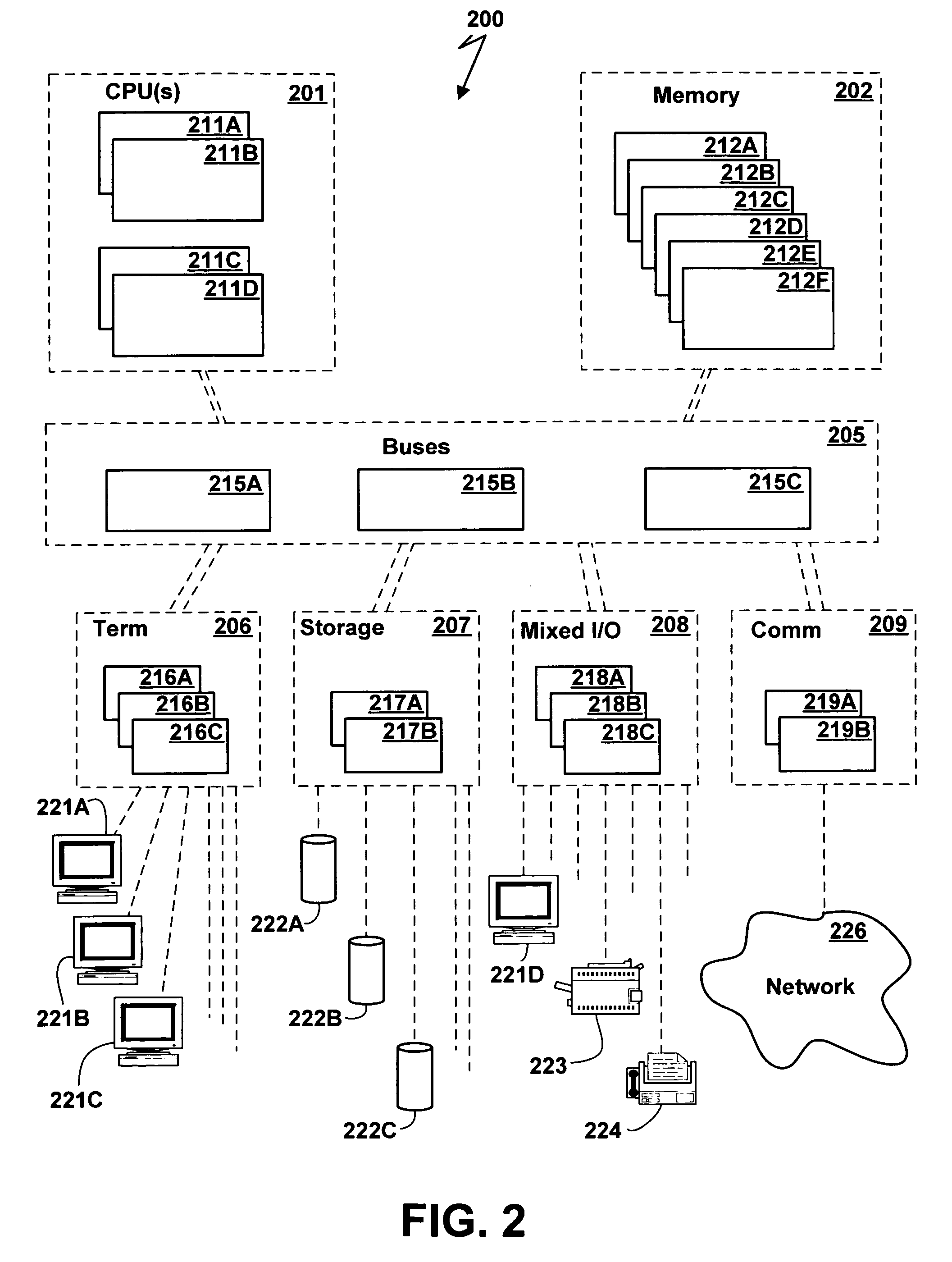
Digital Data Processing Environment

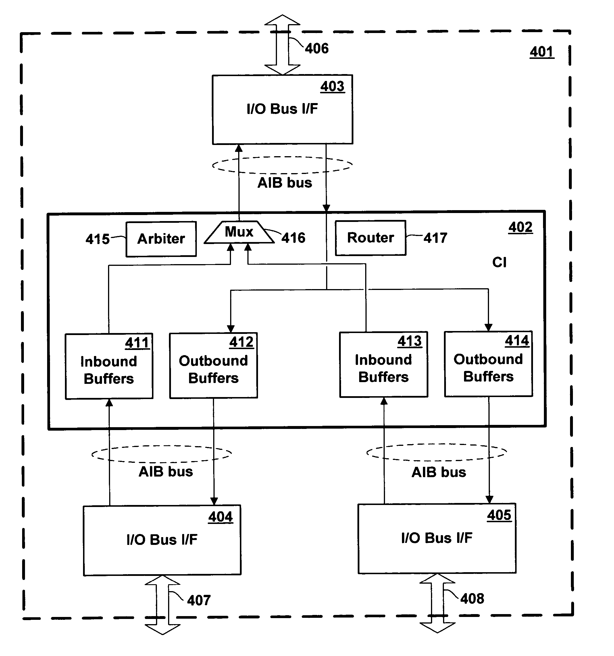
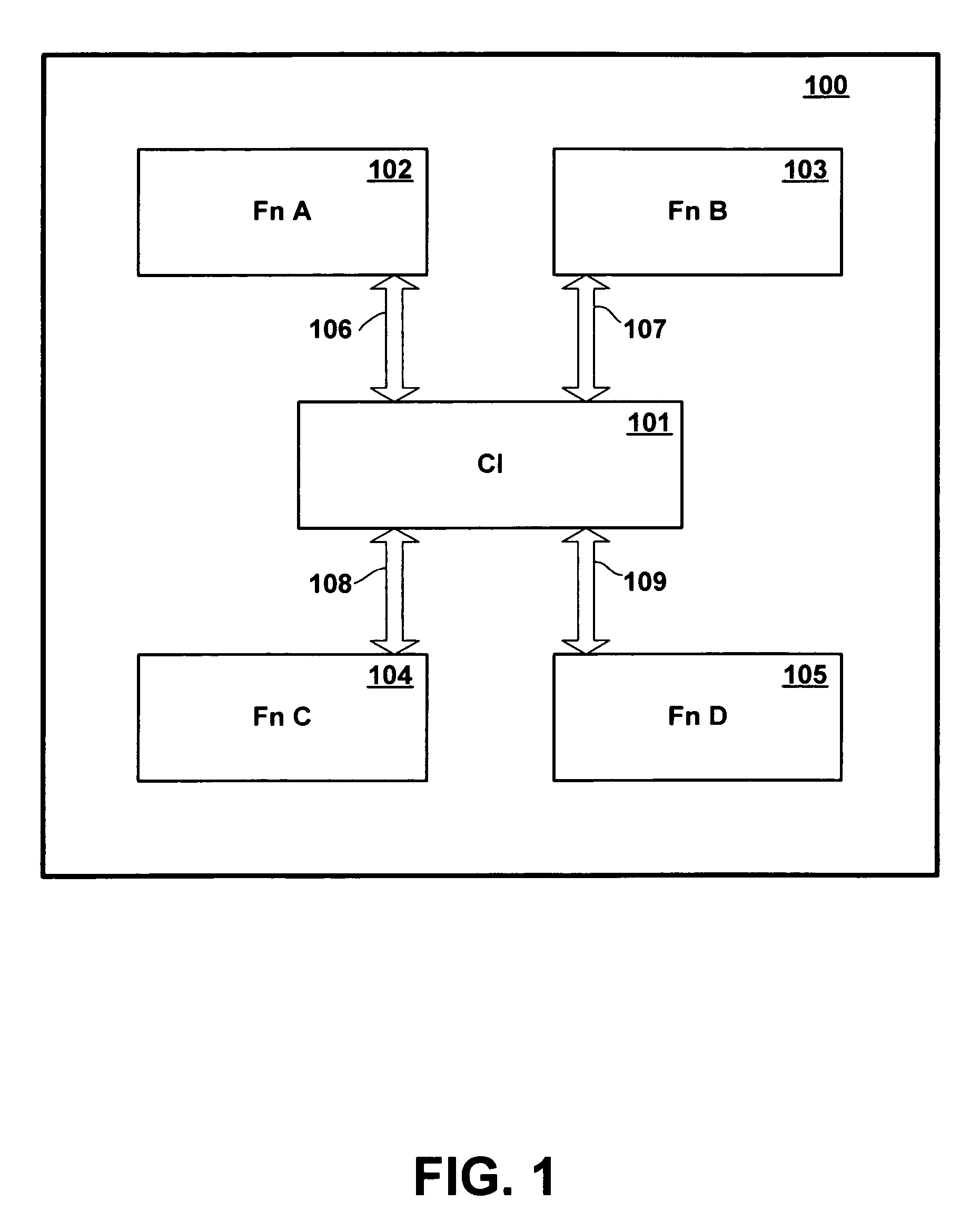
[0042] The present invention relates to the design of digital communications interfaces. In the preferred embodiments, a modular architecture is employed in the design of an integrated circuit chip, whereby a central interconnect module within a chip facilitates data transfer among multiple functional component modules of the chip. Using this architecture, it is possible to design a family of different application specific integrated circuits (ASICs) performing diverse functions, all of which employ a similar central interconnect module design for facilitating internal data transfer. In the exemplary embodiments of the invention described herein, an ASIC performs the function of an I / O bridge interface between different buses of a general-purpose computer system. However, this is but one of many possible implementations and digital data environments in which the present invention might be employed.

[0043] Referring to the Drawing, wherein like nu...


PUM


Abstract

An integrated circuit chip includes multiple functional components and a central interconnect module providing communication among the functional components. The central interconnect module includes a buffer which is shared by the sending and receiving components. Preferably, some components perform different functions and communicate with the central interconnect via a common architectural interface. Preferably, each sender is allocated respective credits representing ability of the receiver to receive data (e.g., available buffer space), and the sender can transmit data if it has credits. Credits are decremented when the sender sends data, and returned by the receiver when is again able to receive. The use of a common central interconnect module with a shared buffer reduces buffer requirements and provides a low-overhead path for transferring data within the integrated circuit chip.

Description

CROSS REFERENCE TO RELATED APPLICATIONS [0001] The present application is related to the following commonly assigned copending applications filed on the same date as the present application, all of which are incorporated by reference: [0002] application Ser. No. ______, entitled “Internal Data Bus Interconnection Mechanism Utilizing Central Interconnection Module Converting Data in Different Alignment Domains” (Assignee's docket number ROC920040240US1); [0003] application Ser. No. ______, entitled “Data Communication Method and Apparatus Utilizing Programmable Channels for Allocation of Buffer Space and Transaction Control” (Assignee's docket number ROC920040241US1); and [0004] application Ser. No. ______, entitled “Data Communication Method and Apparatus Utilizing Credit-Based Data Transfer Protocol and Credit Loss Detection Mechanism” (Assignee's docket number ROC920040281US1).FIELD OF THE INVENTION [0005] The present invention relates to digital data processing hardware, and in p...

Claims


Application Information

Patent Timeline
IPC IPC(8): G06F13/36
CPCG06F13/4059
Inventor CHADHA, SUNDEEPCHECK, MARK ANTHONYDRERUP, BERNARD CHARLESGRASSI, MICHAEL
Owner IBM CORP
Features
  • R&D
  • Intellectual Property
  • Life Sciences
  • Materials
  • Tech Scout
  • Unparalleled Data Quality
  • Higher Quality Content
  • 60% Fewer Hallucinations
Learn More