Method to grow III-nitride materials using no buffer layer

a technology of iiinitride and compound semiconductors, which is applied in the direction of semiconductor devices, basic electric elements, electrical appliances, etc., can solve the problems of limiting the growth conditions of the low t buffer layer, more delays, and extra time and effort, and achieves good surface morphology, high stability, and high crystalline quality.

Inactive Publication Date: 2006-08-10
III N TECH
View PDF3 Cites 64 Cited by
  • Summary
  • Abstract
  • Description
  • Claims
  • Application Information

AI Technical Summary

Benefits of technology

[0014] The present invention provides a method for the growth of nitride materials and devices on sapphire substrate with no buffer layers with high crystalline quality, good surface morphology, high stability, high yield, and good performance. The method includes treating a substrate, e.g., sapphire with a metal. In the preferred embodiment, said metal comprises one of Aluminum, Gallium, Indium, Silicon, and Zirconium from a metalorganic source. Next, high quality nitride materials and devices are grown on the sapphire substrate. Aluminum has been used in the disclosed embodiments. The process avoids the deposition of a buffer layer.

Problems solved by technology

In these methods, however, it is necessary to strictly restrict the growth conditions of the low T buffer layer.
Because the low T buffer layer requires growth conditions which are very different than the subsequent nitride materials, extra time and effort are required.
These added demands create even more delays and require further efforts to optimize the growth conditions of buffer layers and the subsequent nitride materials.

Method used


Image

  • Method to grow III-nitride materials using no buffer layer
  • Method to grow III-nitride materials using no buffer layer
  • Method to grow III-nitride materials using no buffer layer

Examples


example 1

[0039] An AlGaN epitaxial layer was grown to have a film thickness of 2 μm on a sapphire substrate in accordance with the present invention with the following steps.

[0040] First, A sapphire substrate having a diameter of 2 inches was placed on a susceptor.

[0041] Next, the air in reactor was sufficiently exhausted by an exhaust pump, and H2 gas was introduced into the reactor, thus replacing the air in the reactor with H2 gas.

[0042] Thereafter, the susceptor was heated up to 1100° C. by a heater while supplying H2 gas into the reactor. This state was held for around 10 minutes to remove contaminations from the surface of the sapphire substrate.

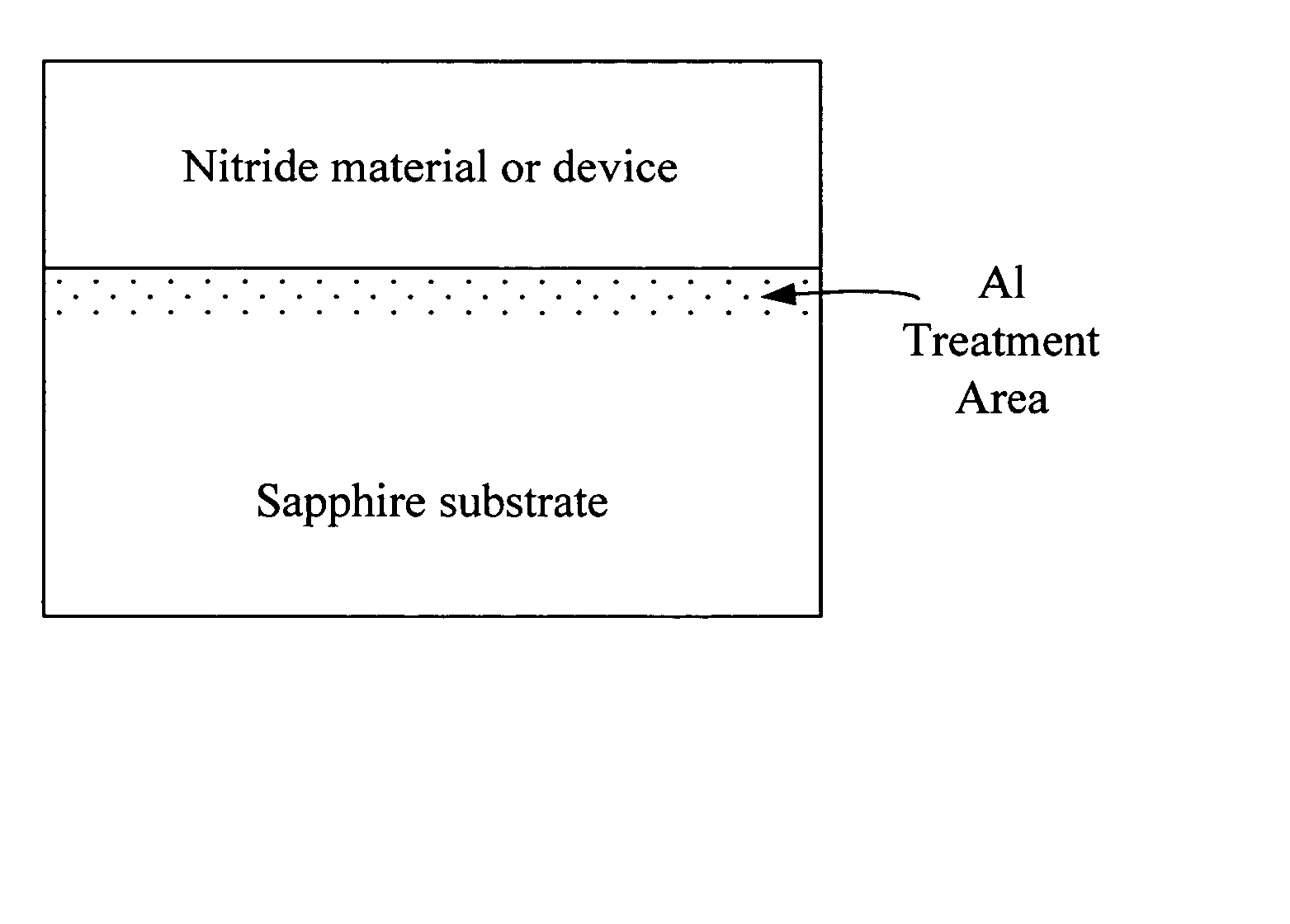
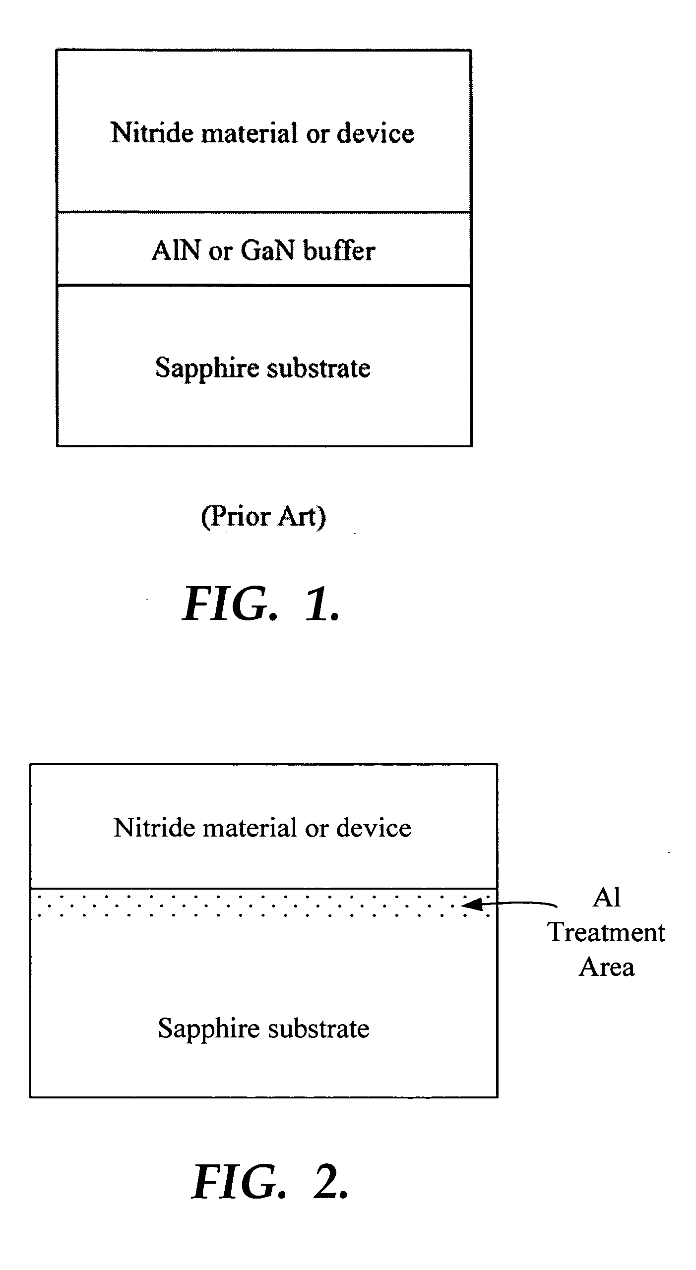
[0043] Subsequently, while maintaining the susceptor at 1100° C., a gas mixture of H2 and TMAl supplied from a metal-organic (MO) source is injected into the reactor for 10 seconds to treat the substrate surface with Aluminum. This results in a modification in the surface state of the sapphire (Al2O3) substrate. The substrate should be subs...

example 2

[0048] An n-GaN was grown on a sapphire substrate in accordance with the present invention with the following steps.

[0049] A sapphire substrate having a diameter of 2 inches was placed on a susceptor.

[0050] Next, the air in reactor was sufficiently exhausted by an exhaust pump, and H2 gas was introduced into the reactor, thus replacing the air in the reactor with H2 gas.

[0051] Thereafter, the susceptor was heated up to 1100° C. by a heater while supplying H2 gas into the reactor. This state was held for 10 minutes to remove contaminations from the surface of the sapphire substrate. The temperature of the susceptor was maintained at 1100° C.

[0052] Subsequently, a gas mixture of H2 and TMAl gas supplied from the MO injection to the reactor for about 2-30 seconds in order that the surface of the substrate is treated with Aluminum. This results in a modification in the surface state of the sapphire (Al2O3) substrate (or results in the substrate being substantially terminated with an...

example 3

[0057] An InGaN / GaN multiple quantum well (MQW) LED structure was grown on a sapphire substrate in accordance with the present invention with the following steps.

[0058] A sapphire substrate having a diameter of 2 inches was placed on a susceptor.

[0059] Next, the air in reactor was sufficiently exhausted by an exhaust pump, and H2 gas was introduced into the reactor, thus replacing the air in the reactor with H2 gas.

[0060] Thereafter, the susceptor was heated up to 1100° C. by a heater while supplying H2 gas into the reactor. This state was held for 10 minutes to remove contaminations from the surface of the sapphire substrate. The temperature of the susceptor was maintained at 1100° C.

[0061] Subsequently, a gas mixture of H2 and TMAl gas was supplied via MO injection to the reactor for about 2-30 seconds to treat the substrate surface with Al. This resulted in a modification in the surface state of the sapphire (Al2O3) substrate. Thus, the substrate was substantially terminated ...


PUM

PropertyMeasurementUnit
thicknessaaaaaaaaaa
temperatureaaaaaaaaaa
thicknessaaaaaaaaaa

Abstract

Disclosed is a method for growing nitride compound semiconductors on sapphire substrates where no low-temperature buffer layer is used. The nitride based compound semiconductor materials and devices grown by the method of the present invention have crystallinity and surface morphology at practical levels with high quality, high stability, and high yield.

Description

CROSS-REFERENCE TO RELATED APPLICATIONS [0001] This application claims the benefit of U.S. Provisional Application No. 60 / 650,929 filed Feb. 8, 2005 under the same title.STATEMENT REGARDING FEDERALLY SPONSORED RESEARCH OR DEVELOPMENT [0002] The U.S. Government has a paid-up license in this invention and the right in limited circumstances to require the patent owner to license others on reasonable terms as provided for by the Contract No. DMI-0450314 awarded by the National Science Foundation.BACKGROUND OF THE INVENTION [0003] 1. Field of the Invention [0004] The present invention relates to the field of growing III-nitride-based compound semiconductor materials and devices epitaxially on substrates (e.g., sapphire) and particularly, to a method of growing high-quality III-nitride-based compound semiconductor materials and devices without using a buffer layer. [0005] 2. Description of the Related Art [0006] The III-nitride semiconductors have recently been the focus of intense resear...

Claims


Application Information

Patent Timeline
Patent Type & Authority Applications(United States)
IPC IPC(8): H01L29/12
CPCH01L21/0242H01L21/02491H01L21/0254H01L21/02576H01L21/02579H01L21/0262H01L21/02658
Inventor LI, JING
Owner III N TECH
Why Eureka
Try Eureka