Semiconductor device having semiconductor chips stacked and mounted thereon and manufacturing method thereof

a semiconductor chip and semiconductor technology, applied in semiconductor devices, semiconductor/solid-state device details, electrical devices, etc., can solve the problems of difficult to deal with the wafer, easy to crack or chip cracking, and easy to chip cracking

Active Publication Date: 2006-08-10
KIOXIA CORP
View PDF9 Cites 137 Cited by
  • Summary
  • Abstract
  • Description
  • Claims
  • Application Information

AI Technical Summary

Benefits of technology

[0020] A semiconductor device according to an aspect of this invention comprises a plurality of semiconductor chips which are stacked and mounted on a circuit board having external connection electrodes and each of which is mounted on the circuit board by means of wire bonding, wherein at least one semiconductor chip stacked on the semiconductor chip includes bonding pads which are arranged on a main surface of the semiconductor chip along at least one side thereof and electrically connected to semiconductor elements, overhung portions formed in positions of a backside of the semiconductor chip corresponding to the bonding pads, having a start point inside the bonding pads, formed to become thinner in a direction toward an outer periphery to an end point which reaches a side wall thereof, and forming spaces to accommodate ball bonding portions between the overhung portions and a main surface of a semiconductor chip arranged in a lower stage, and insulating layers which are formed to cover the overhung portions and prevent the chip from being brought into contact with bonding wires of the semiconductor chip arranged in the lower stage.

Problems solved by technology

However, with the above structure and manufacturing method, the following problems (1) to (6) are provided.
(1) If the semiconductor wafer is diced with the DAF affixed thereon after the backside of the semiconductor wafer is ground, etched or the like to reduce the thickness thereof to desired thickness, chippings or cracks often occur on the backside of the chip.
(2) If the thickness of the semiconductor wafer is set to 70 μm or less, breakage of the wafer tends to occur and it becomes difficult to deal with the wafer.
Therefore, it is not only difficult to deal with the chip, but also a recognition error occurs at the time of position detection by using an optical system such as a TV camera performed when the chip is stacked and mounted.
(3) Chip cracks often occur when individual semiconductor chips are picked up (separated) from a dicing tape after the semiconductor wafer is divided into the discrete chips.
Further, when the thickness of the semiconductor chip becomes less than 100 μm, deflection (bending) occurs in the semiconductor chip when it is attracted by a collet and voids occur in the die-bonding (adhesion and pressure-connection) process.
(4) The semiconductor chip of the second stage or succeeding state is bent by pressurization at the ball bonding time because no rigid material is present under the bonding pad and the chip itself is thin and a lowering in the bonding property, for example, a loose connection and faulty connection position tend to occur.
Further, if the bending amount of the chip is further increased, wire deformation and chip cracks occur in the semiconductor chip of the lower layer.
(5) When the semiconductor chips of the same size are stacked or the semiconductor chips of different sizes including a chip of the upper stage larger than the chip of the lower stage are stacked in the second and succeeding stages, it is necessary to dispose a spacer and DAF between the semiconductor chips and the package thickness cannot be made sufficiently small even if the semiconductor chip is made sufficiently thin.
If the spacer and DAF are made thin, a short circuit or leak tends to occur between the bonding wire and the backside of the semiconductor chip stacked in the upper stage.
Further, there occurs a possibility that the bonding wire flows to cause a short circuit at the time of resin-sealing.
(6) Costs for fabricating and bonding processes are necessary in addition to a material cost for the spacer and DAF, and as a result, the cost increases and the productivity is lowered.
However, the above structure and manufacturing method have the following problems (7) to (10).
(7) If the semiconductor wafer is diced after the backside of the semiconductor wafer is ground and etched and the thickness of the wafer is reduced to desired thickness, chippings and cracks often occur on the backside of the chip.
(8) If the thickness of the semiconductor wafer is set to 70 μm or less, breakage tends to occur and it is difficult to deal with the wafer.
Therefore, it is not only difficult to deal with the chip, but also a recognition error occurs at the time of position detection performed by using an optical system such as a TV camera when the chip is stacked and mounted.
(9) Chip cracks often occur when individual semiconductor chips are picked up (separated) from a dicing tape after the semiconductor wafer is divided into the discrete chips.
Further, when the thickness of the semiconductor chip becomes less than 100 μm, deflection (bending) occurs in the semiconductor chip when it is attracted by a collet and voids occur in the die bonding process.

Method used


Image

  • Semiconductor device having semiconductor chips stacked and mounted thereon and manufacturing method thereof
  • Semiconductor device having semiconductor chips stacked and mounted thereon and manufacturing method thereof
  • Semiconductor device having semiconductor chips stacked and mounted thereon and manufacturing method thereof

Examples


first embodiment

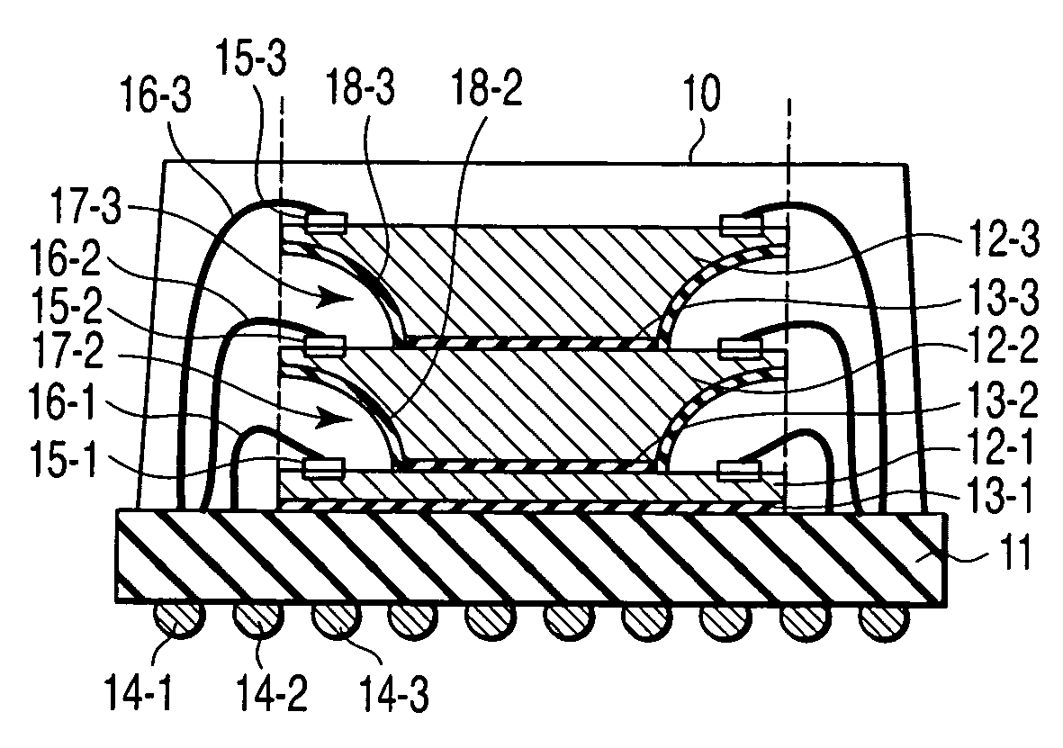
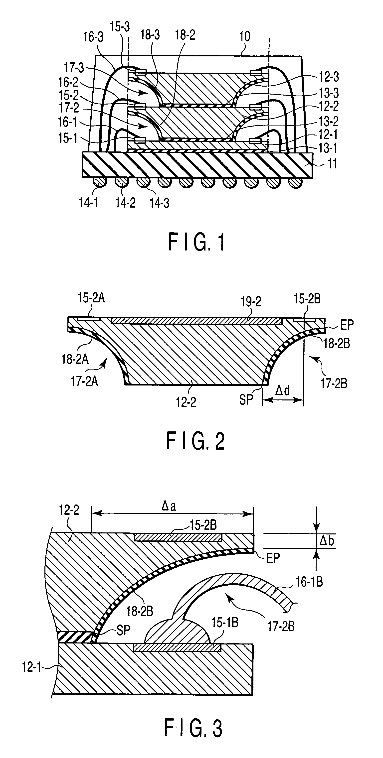
[0168]FIG. 1 is a cross sectional view showing a semiconductor device according to a first embodiment of this invention. In this case, a stack MCP having three semiconductor chips with the same size stacked is dealt with as an example. That is, three semiconductor chips 12-1, 12-2, 12-3 with the same size are stacked and mounted on a printed circuit board (PCB) 11 with DAFs 13-1, 13-2, 13-3 disposed therebetween, respectively. For example, the circuit board 11 has a multi-layered wiring structure. Wirings to which bonding wires are connected are formed on the chip mounting surface of the circuit board 11 and external connection electrodes (external terminals) 14-1, 14-2, 14-3, . . . such as ball bumps (solder balls) and pins are arranged in an array form on the backside thereof to form a so-called ball grid array or pin grid array.

[0169] Bonding pads 15-1, 15-2, 15-3 formed on the main surfaces of the semiconductor chips 12-1, 12-2, 12-3 and the printed wirings formed on the chip m...

second embodiment

[0320]FIG. 124 is a cross sectional view of a semiconductor device according to a second embodiment of this invention. In this case, a COC package type semiconductor device having three semiconductor chips with the same size stacked is taken as an example. Three semiconductor chips 12-1, 12-2, 12-3 with the same size are stacked and mounted on a circuit board 11 with DAFs (die attach films) 13-1, 13-2, 13-3 disposed therebetween, respectively. For example, the circuit board 11 has a multi-layered wiring structure. Electrode pads on which stud bumps 56-1 are formed are provided on the chip mounting surface of the circuit board 11 and external connection electrodes 14-1, 14-2, 14-3, . . . such as solder balls and pins are arranged in an array form on the backside of the chip to form a so-called ball grid array or pin grid array.

[0321] Through electrodes 55-1, 55-2, 55-3 formed of copper (Cu), gold (Au), tungsten (W) or polysilicon are provided along the two (or four) opposite sides o...

an example 1

of the Process of Filling Spaces with Insulating Members

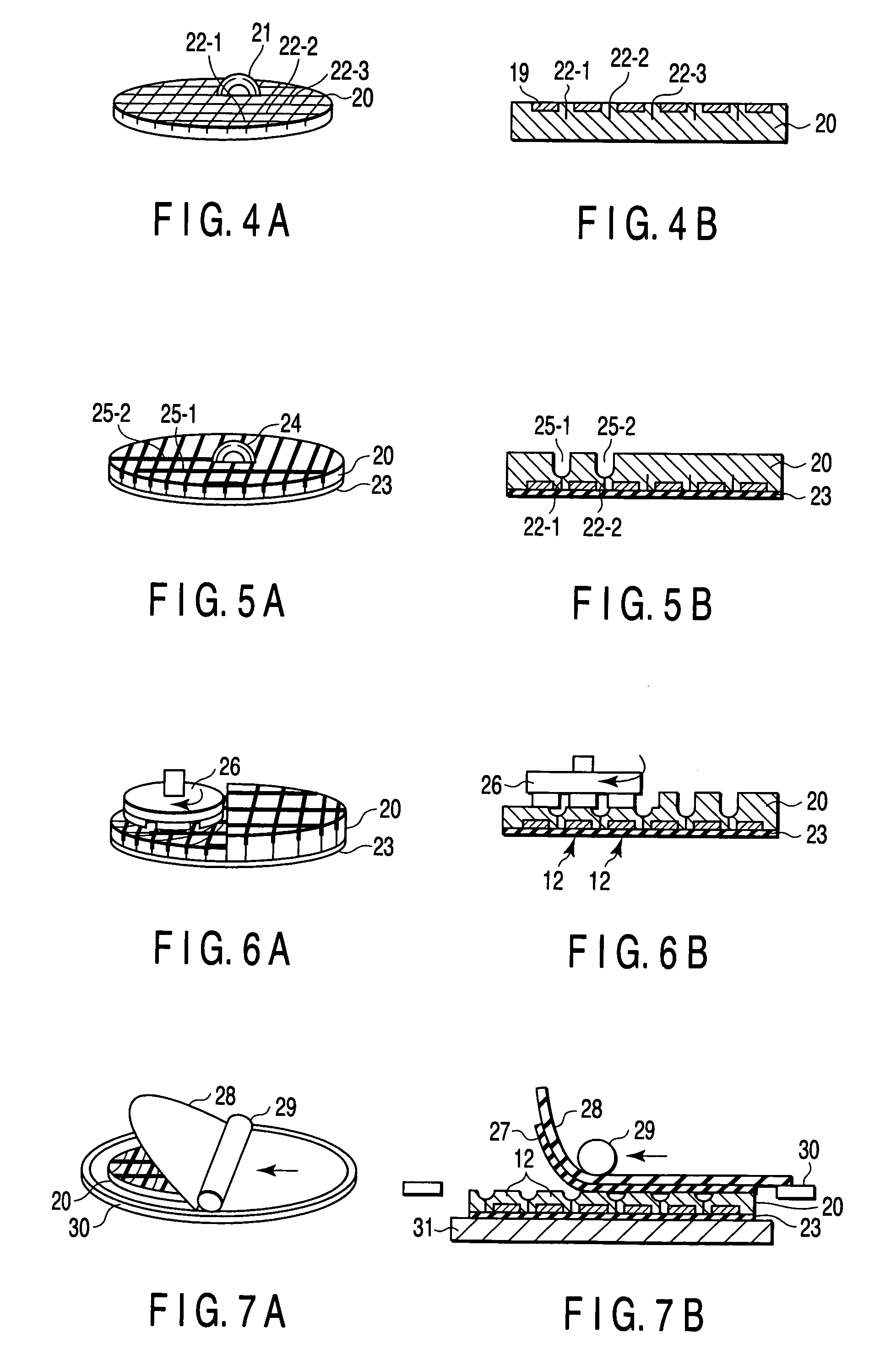
[0461]FIGS. 196A, 196B show an example of the process of filling spaces under the overhung portions with insulating members. The process shown in FIGS. 196A, 196B is to mount a chip by use of a DAF and fill spaces with insulating members and shows a state in which a first-stage chip 12-1 is mounted on a circuit board 11. An insulating material such as an insulating bonding agent or sealing resin is supplied from a dispenser nozzle 36 onto connection electrodes (in this example, ball bumps 42-2 are shown as an example) of the chip 12-1. A semiconductor chip 12-2 formed in the above process is stacked and mounted on the chip 12-1 with a DAF disposed therebetween. When the chip 12-2 is stacked and mounted on the chip 12-1, the overhung portions thereof are set to correspond in position to the ball bumps 42-2 of the chip 12-1 arranged in the lower stage. Thus, spaces formed between the main surface of the chip 12-1 arranged in the ...


PUM


Abstract

Chips are stacked and mounted on a circuit board having external connection electrodes and mounted thereon by wire bonding. At least one of the chips stacked on the chip includes overhung portions each of which has a start point inside bonding pads, is made thinner in a direction towards the outer periphery to an end point reaching the side wall and forms a space used to accommodate ball bonding portions between the overhung portion and the main surface of the chip arranged in the lower stage on a backside corresponding in position to the bonding pads, and insulating members formed to cover the overhung portions and prevent bonding wires of the chip arranged in the lower stage from being brought into contact with the upper-stage chip.

Description

CROSS-REFERENCE TO RELATED APPLICATIONS [0001] This application is based upon and claims the benefit of priority from prior Japanese Patent Applications No. 2005-026698, filed Feb. 2, 2005; and No. 2005-026699, filed Feb. 2, 2005, the entire contents of both of which are incorporated herein by reference. BACKGROUND OF THE INVENTION [0002] 1. Field of the Invention [0003] This invention relates to a semiconductor device having semiconductor chips stacked and mounted thereon and a manufacturing method thereof. More specifically, this invention relates to a package type semiconductor device of next generation called a COC (Chip On Chip) and a manufacturing method thereof and a semiconductor device called a stacked MCP (Multi-Chip Package) having the stacked and mounted semiconductor chips sealed in one package and a manufacturing method thereof. [0004] 2. Description of the Related Art [0005] A stacked MCP in which the chip thickness and the package thickness are reduced is described i...

Claims


Application Information

Patent Timeline
Patent Type & Authority Applications(United States)
IPC IPC(8): H01L23/02H01L21/50
CPCH01L21/6836H01L23/481H01L24/27H01L24/48H01L24/83H01L24/85H01L25/0657H01L25/50H01L29/0657H01L2221/68327H01L2221/6834H01L2224/05644H01L2224/05647H01L2224/05684H01L2224/13144H01L2224/29012H01L2224/32145H01L2224/32225H01L2224/48091H01L2224/48227H01L2224/48465H01L2224/73265H01L2224/83191H01L2224/83194H01L2224/838H01L2224/8592H01L2224/92247H01L2225/0651H01L2225/06517H01L2225/06541H01L2225/06555H01L2225/06572H01L2225/06582H01L2924/01014H01L2924/01029H01L2924/01057H01L2924/01079H01L2924/014H01L2924/15311H01L24/29H01L2224/2919H01L2924/00014H01L2924/01005H01L2924/01033H01L2924/01074H01L2924/01075H01L2924/0665H01L2224/0401H01L2924/00H01L2224/45099H01L2924/3512H01L2924/00012H01L2924/10155H01L2924/181H01L24/73
Inventor KUROSAWA, TETSUYASAGARA, JUNYA
Owner KIOXIA CORP
Why Eureka
Try Eureka