Operational amplifier circuit

a technology of operating amplifier circuit and amplifier circuit, which is applied in the direction of dc-amplifiers with dc-coupled stages, differential amplifiers, and amplifiers with semiconductor devices/discharge tubes, etc., can solve the problems of unstable operation of the operating amplifier circuit, dc gain cannot be increased, and considerable deterioration of the band characteristics of the operational amplifier circuit, etc., to achieve high dc gain, improve dc gain, and improve the effect of gain

Inactive Publication Date: 2006-08-10
RENESAS ELECTRONICS CORP
View PDF4 Cites 5 Cited by
  • Summary
  • Abstract
  • Description
  • Claims
  • Application Information

AI Technical Summary

Problems solved by technology

However, a gate-source capacitance of the non-doped Nch transistor is very large and thus functions as a load of the input circuit part, leading to considerable deterioration of band characteristics of the operational amplifier circuit.
If the secondary pole is shifted to the lower frequency side, there arises a problem that an operation of the operational amplifier circuit becomes unstable.
As a result, the operational amplifier circuit of FIG. 2 has a drawback that the DC gain cannot be increased.
However, this results in an increase in element area and power consumption.
Hence, the insertion of the Pch transistor to the signal amplifying path is undesirable in terms of wide-band characteristics.
Thus, a problem about reduction in power supply voltage down to about 1.5 V and a problem about reduction in frequency band for amplified differential signal components are solved.
However, a channel width of the non-doped Nch transistor for generating a bias voltage needs to increase for operating the transistor at a power supply voltage lower than 1.5 V. Thus, there arises a problem that an area of the non-doped Nch transistor in a semiconductor chip increases, which hinders size reduction of the semiconductor chip.

Method used


Image

  • Operational amplifier circuit
  • Operational amplifier circuit
  • Operational amplifier circuit

Examples


Embodiment Construction

[0021] The invention will be now described herein with reference to illustrative embodiments. Those skilled in the art will recognize that many alternative embodiments can be accomplished using the teachings of the present invention and that the invention is not limited to the embodiments illustrated for explanatory purposed.

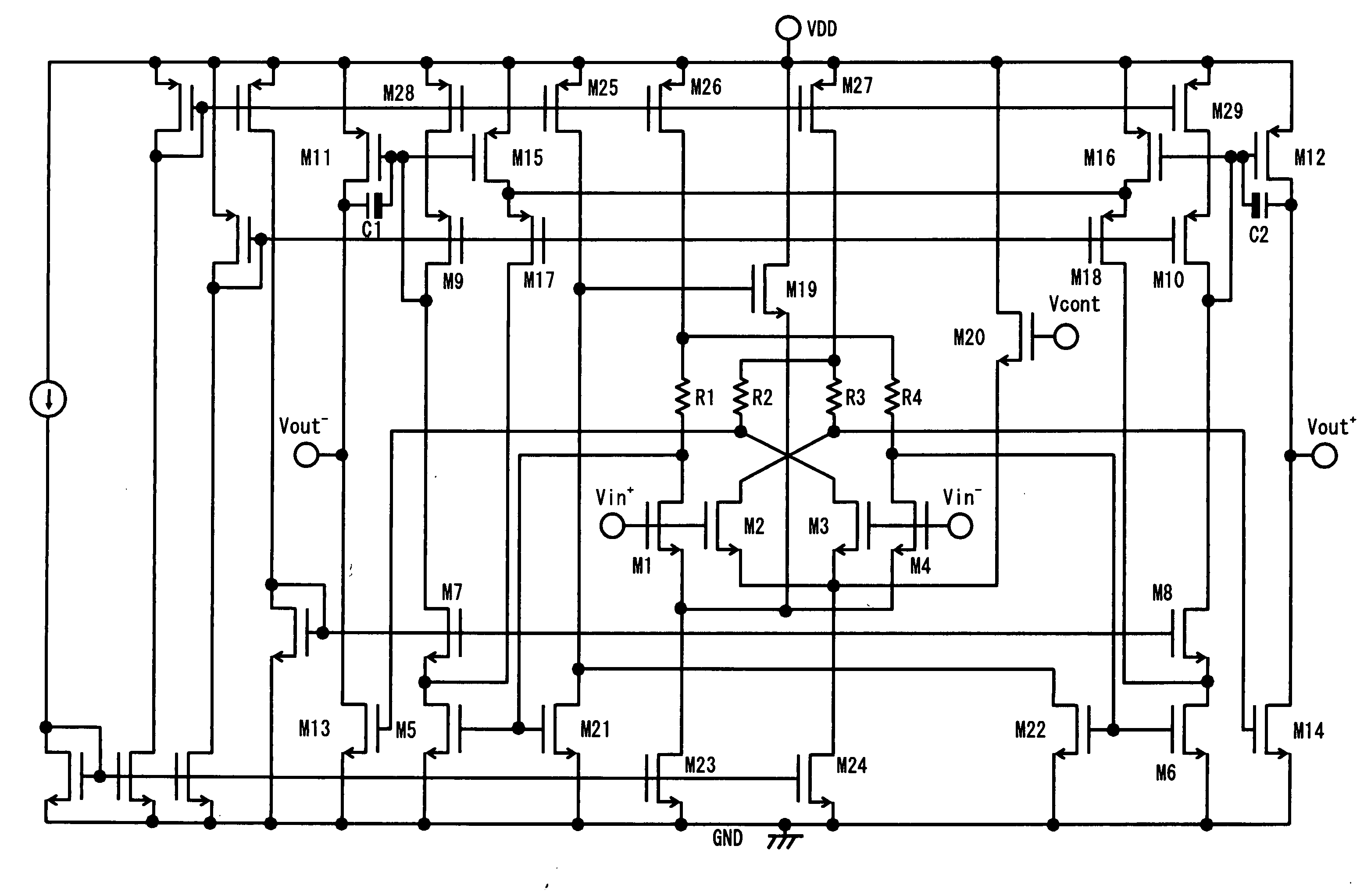
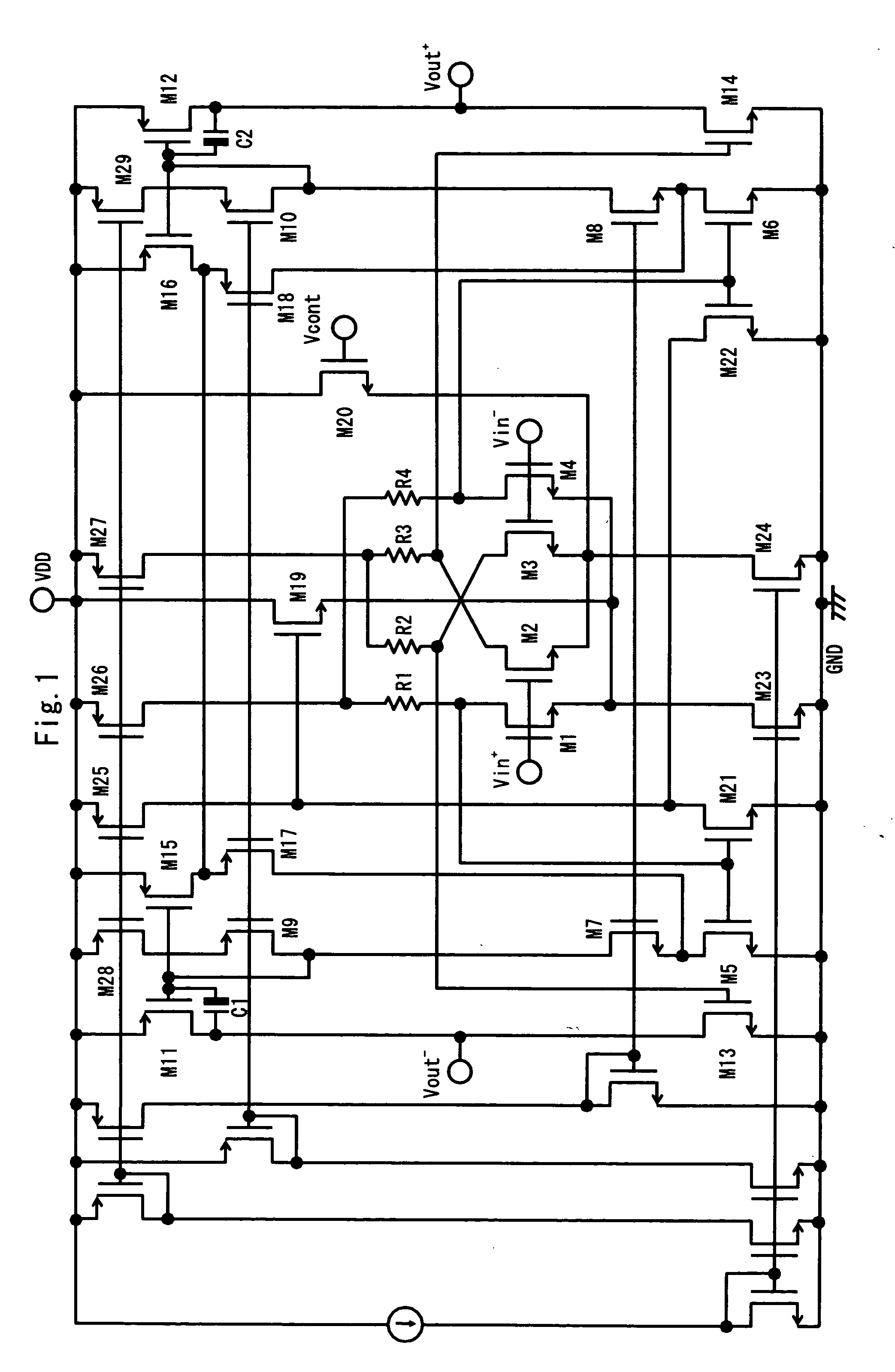
[0022]FIG. 1 is a circuit diagram showing an operational amplifier circuit according to an embodiment of the present invention. As shown in FIG. 1, first and second Nch transistors (for example, Nch transistors M1 and M4) make a first differential transistor pair. Gate electrodes of the first differential transistor pair are applied with differential input signals Vin+ and Vin−, respectively. Source electrodes thereof are commonly connected with a drain electrode of a first constant current source Nch transistor (for example, constant current source transistor M23). Drain electrodes thereof are connected with one terminals of first and second load resistors (fo...


PUM


Abstract

To provide a differential operational amplifier circuit that attains a wide-band and high-DC-gain characteristic and operates with a low power supply voltage. A signal path having three amplifier circuits passing an Nch transistor pair, cascode connected Nch transistor pairs, and a Pch transistor pair functions as a gain path having a high-gain and narrow-band characteristic. In addition, a signal path having two amplifier circuits passing an Nch transistor pair and another Nch transistor pair functions as a feedforward path having a low-gain and wide-band characteristic. Signals amplified through each path are synthesized at an output terminal, whereby a high-gain and wide-band operational amplifier is attained. Further, a constant current source transistor pair supplies a constant current to four drain load resistors of a first differential amplifying pair to drive a circuit with a constant current, thereby reducing a power supply voltage.

Description

BACKGROUND OF THE INVENTION [0001] 1. Field of the Invention [0002] The present invention relates to a differential operational amplifier circuit, and more particularly to a high-gain and wide-band operational amplifier circuit. [0003] 2. Description of Related Art [0004] As an example of differential operational amplifier circuits, an operational amplifier circuit composed of an input circuit including a differential transistor pair and an output circuit including a cascode circuit is described in “Analog Integrated Circuits and Signal Processing, vol. 18, pp. 21-31 (1999)” and “IEEE Journal of Solid-State Circuits, Vol. 30, No. 3, March 1995, pp. 166-172”. FIG. 2 is a circuit diagram showing the example of the operational amplifier circuit described in the above document. The operational amplifier circuit of FIG. 2 is composed of a wide-band differential input circuit including Nch transistors M1 to M4 and a differential output circuit including a cascode circuit of Nch transistor...

Claims


Application Information

Patent Timeline
Patent Type & Authority Applications(United States)
IPC IPC(8): H03G3/18
CPCH03F3/3022H03F3/45183H03F2203/30021H03F2203/45366
Inventor ETOU, TOSHIYUKI
Owner RENESAS ELECTRONICS CORP
Why Eureka
Try Eureka