Interposer for decoupling integrated circuits on a circuit board

Active Publication Date: 2006-08-10
ALCATEL LUCENT SAS
View PDF9 Cites 8 Cited by
  • Summary
  • Abstract
  • Description
  • Claims
  • Application Information

AI Technical Summary

Benefits of technology

[0009] In this interposer, capacitors are easily formed by connecting metal structures from the first set to the top metal layer and adjacent metal structures from the second set to

Problems solved by technology

These capacitors, however, consume surface area on the circuit board and hence limit the achievable integration density.
However, since the surface a

Method used


Image

  • Interposer for decoupling integrated circuits on a circuit board
  • Interposer for decoupling integrated circuits on a circuit board
  • Interposer for decoupling integrated circuits on a circuit board

Examples


Embodiment Construction

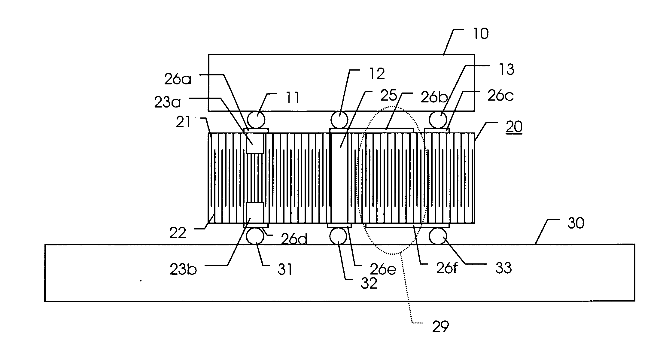
[0018] A first embodiment of the invention is shown schematically as a cross-section in FIG. 1. A Ball Grid Array (BGA) packaged microchip 10 is attached on an interposer 20, which is fastened on a printed circuit board 30. The microchip has three solder balls 11, 12, and 13 on its bottom side, which connect to corresponding solder pads 26a, 26b, and 26c on the top surface of the interposer. Solder balls 31, 32, and 33 on the circuit board 30 connect to corresponding solder pads 26d, 26e, and 26f on the bottom surface of the interposer 20.

[0019] The interposer 20 itself contains vertical metal structures 21, 22 of alternating type. A first set of metal structures 21 extends towards the top surface layer of the interposer 20 and a second set of metal structures 22 extends towards the bottom surface of the interposer 20. Solder pads 26b and 26c hence connect to some of the upper metal structures 21, while solder pad 26f for instance connects to some of the lower metal structures 22. ...


PUM


Abstract

An interposer (20) is used for decoupling a microchip (10) on a circuit board (30). The interposer (20) contains on its upper and lower surfaces structured metal layers (26a-26d) for attachment to the microchip (10) and the circuit board (30), respectively. Inside the interposer, there are two sets of mutually isolated metal structures (21, 22) extending substantially perpendicular to the upper and lower surfaces of said interposer (20). The first set (21) extends closer towards the upper surface than the second set (22), while said second set (22) extends closer towards the lower surface than said first set (21).

Description

[0001] The invention is based on a priority application EP 05290242.6 which is hereby incorporated by reference. FIELD OF THE INVENTION [0002] The present invention relates to the field of electronics and more particular to an interposer for use on a printed circuit board for decoupling integrated circuits. BACKGROUND OF THE INVENTION [0003] As the level of integration increases, the number of pins of a integrated circuit package that need to be connected to a circuit board becomes larger and larger. A well known packaging technique is called Ball Grid Array (BGA), which is a type of microchip connection methodology. A Ball Grid Array chip is a square package with solder balls on the underside for surface mounting. Use of BGA allows die package size to be reduced by allowing more surface area for attachment. Smaller packaging allows more components to be mounted on a module making greater densities available. [0004] On the other hand, the clock rate under which modern integrated cir...

Claims


Application Information

Patent Timeline
IPC IPC(8): H05K7/06H05K1/11
CPCH01G4/232H01L23/49827H01L23/50H01L2224/16H01L2924/0102H01L2924/01079H01L2924/15311H01L2924/19103H05K1/0231H05K1/162H05K2201/10378H01L2924/10253H01L2924/00H01L2224/16227H01L2224/16235
Inventor HOFFMANN, HANSWOLFEL, WERNER
Owner ALCATEL LUCENT SAS
Why Eureka
Try Eureka