Vertical stacking of multiple integrated circuits including SOI-based optical components

a technology of optical components and vertical stacking, which is applied in the direction of optical elements, instruments, optical waveguide light guides, etc., can solve the problems of large bow to wafers, high cost, and high cost of soi-based structure for fine line electronics

Inactive Publication Date: 2006-08-10
SIOPTICAL INC +1
View PDF12 Cites 81 Cited by
  • Summary
  • Abstract
  • Description
  • Claims
  • Application Information

AI Technical Summary

Benefits of technology

[0006] It is an aspect of the present invention that by separating the electrical components and opto-electronic components onto separate ICs, each can be optimized independently, while maintaining interconnection therebetween.
[0007] A further aspect of the present invention is th

Problems solved by technology

While this finer linewidth photolithography is acceptable for electronic applications, it presents problems for silicon-on-insulator (SOI) applications that attempt to incorporate optical devices within the same structure as the electronics.
However, having a one micron thick bu

Method used


Image

  • Vertical stacking of multiple integrated circuits including SOI-based optical components
  • Vertical stacking of multiple integrated circuits including SOI-based optical components
  • Vertical stacking of multiple integrated circuits including SOI-based optical components

Examples


Embodiment Construction

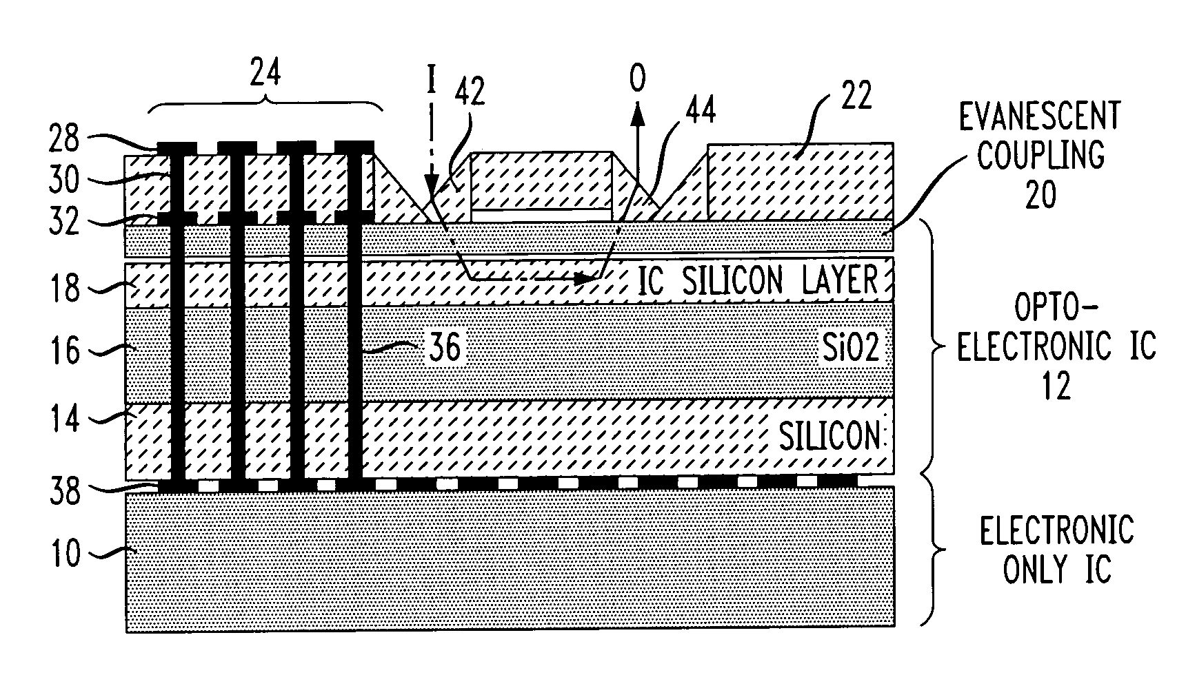
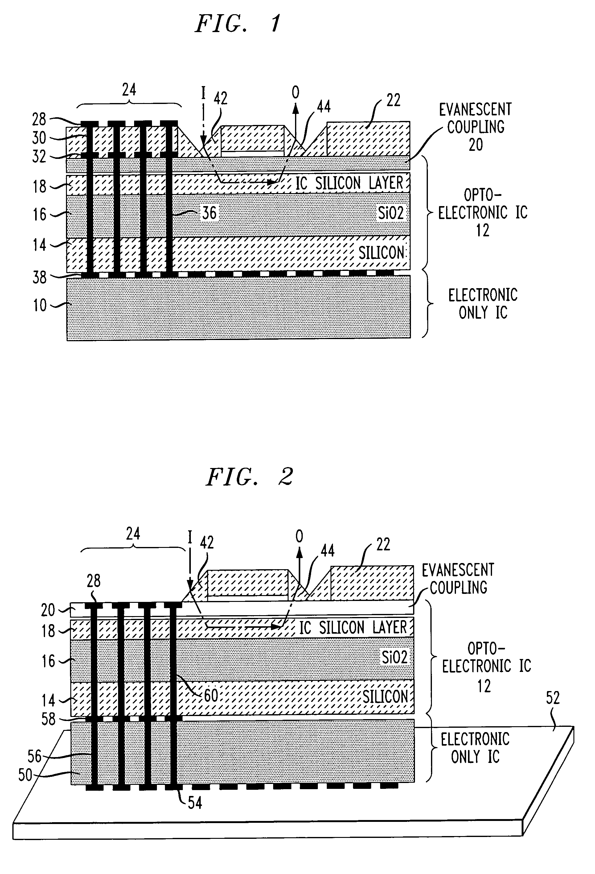
[0018]FIG. 1 illustrates, in a cut-away side view, an exemplary vertical stack arrangement formed in accordance with the present invention. As shown, the arrangement includes a first integrated circuit (IC) 10 comprising electronic circuitry, where IC 10 is fabricated using conventional CMOS processing techniques. Indeed, fine linewidth lithography as described above may be used to form the elements within IC 10. An SOI-based opto-electronic circuit 12 is disposed over electronic IC 10 in the manner shown in FIG. 1. As is well-known in the art, SOI-based circuit 12 includes a base silicon substrate 14, a buried oxide layer 16 and relatively thin silicon surface layer 18 (hereinafter referred to as an “SOI layer”). Although not particularly illustrated in FIG. 1 for the sake of clarity, this layer may include various doping regions and / or other sub-layers (such as polysilicon, interlevel dielectrics and metallizations) as required to form the desired passive and active optical device...


PUM


Abstract

A vertical stack of integrated circuits includes at least one CMOS electronic integrated circuit (IC), an SOI-based opto-electronic integrated circuit structure, and an optical input/output coupling element. A plurality of metalized vias may be formed through the thickness of the stack so that electrical connections can be made between each integrated circuit. Various types of optical input/output coupling can be used, such as prism coupling, gratings, inverse tapers, and the like. By separating the optical and electrical functions onto separate ICs, the functionalities of each may be modified without requiring a re-design of the remaining system. By virtue of using SOI-based opto-electronics with the CMOS electronic ICs, a portion of the SOI structure may be exposed to provide access to the waveguiding SOI layer for optical coupling purposes.

Description

CROSS-REFERENCE TO RELATED APPLICATION [0001] This application claims the benefit of US Provisional Application No. 60 / 650,061, filed Feb. 4, 2005.TECHNICAL FIELD [0002] The present invention relates to a vertically stacked packaging arrangement for multiple integrated circuit chips and, more particularly, to a vertical stacking arrangement for use with SOI-based optical components and associated electronic integrated circuits. BACKGROUND OF THE INVENTION [0003] Today's standard CMOS lithography design rules for electronic integrated circuits (ICs) utilize a linewidth of 90 nm, with the very likely possibility of being reduced going forward to 65 nm and below, perhaps down to a fine linewidth on the order of 22-32 nm (or less). While this finer linewidth photolithography is acceptable for electronic applications, it presents problems for silicon-on-insulator (SOI) applications that attempt to incorporate optical devices within the same structure as the electronics. In particular, th...

Claims


Application Information

Patent Timeline
IPC IPC(8): G02B6/12G02B6/26G02B6/42G02B6/10
CPCG02B6/42G02B6/4214G02B6/43G02F1/025H01L31/12
Inventor SHASTRI, KALPENDUPATEL, VIPULKUMARPIEDE, DAVIDFANGMAN, JOHN
Owner SIOPTICAL INC
Why Eureka
Try Eureka