Luminescence device and display apparatus

a luminescent device and display device technology, applied in the direction of discharge tube luminescent screen, other domestic articles, natural mineral layered products, etc., can solve the problems of material change or life deterioration, material change or deactivation process, and limited luminescence efficiency to at most 25%, and achieve high luminescence efficiency, long device life, and high stability as luminescent materials.

Inactive Publication Date: 2006-08-10
CANON KK
View PDF25 Cites 33 Cited by
  • Summary
  • Abstract
  • Description
  • Claims
  • Application Information

AI Technical Summary

Benefits of technology

[0034] Accordingly, a principal object of the present invention is to provide a compound capable of high efficiency luminescence and showing a high stability as a luminescent material for use in a phosphorescent luminescence device. Particularly, it is an object to provide a luminescence material compound which is less liable to cause energy deactivation in a long life of excited energy state and is also chemically stable, thus providing a longer device life. A further object of the present invention is to provide a red luminescence material compound capable of emitting pure red suitable for forming a full-color display device.
[0035] Inclusively, principal objects of the present invention are to provide a luminescence material which exhibits a high luminescence efficiency, retains a high luminance for a long period and is capable of red luminescence based on phosphorescent luminescence materials, and also provide a luminescence device and a display apparatus using the same.

Problems solved by technology

Conventional organic EL devices have utilized fluorescence of which the luminescence efficiency is limited to at most 25%.
More specifically, because it is held in a high-energy excited state for a longer period, it is liable to react with surrounding materials and cause polymer formation among the excitons, thus incurring a higher probability of deactivation process resulting in a material change or life deterioration.
Further, in view of the formation of a full-color display device, luminescence materials providing luminescence colors which are as close as possible to pure three primary colors of blue, green and red, are desired, but there have been few luminescence materials giving a luminescence color of pure red, so that the realization of a good full-color display device has been restricted.

Method used


Image

  • Luminescence device and display apparatus
  • Luminescence device and display apparatus
  • Luminescence device and display apparatus

Examples


examples

[0182] Hereinbelow, the present invention will be described more specifically based on Examples.

examples 1 and 2

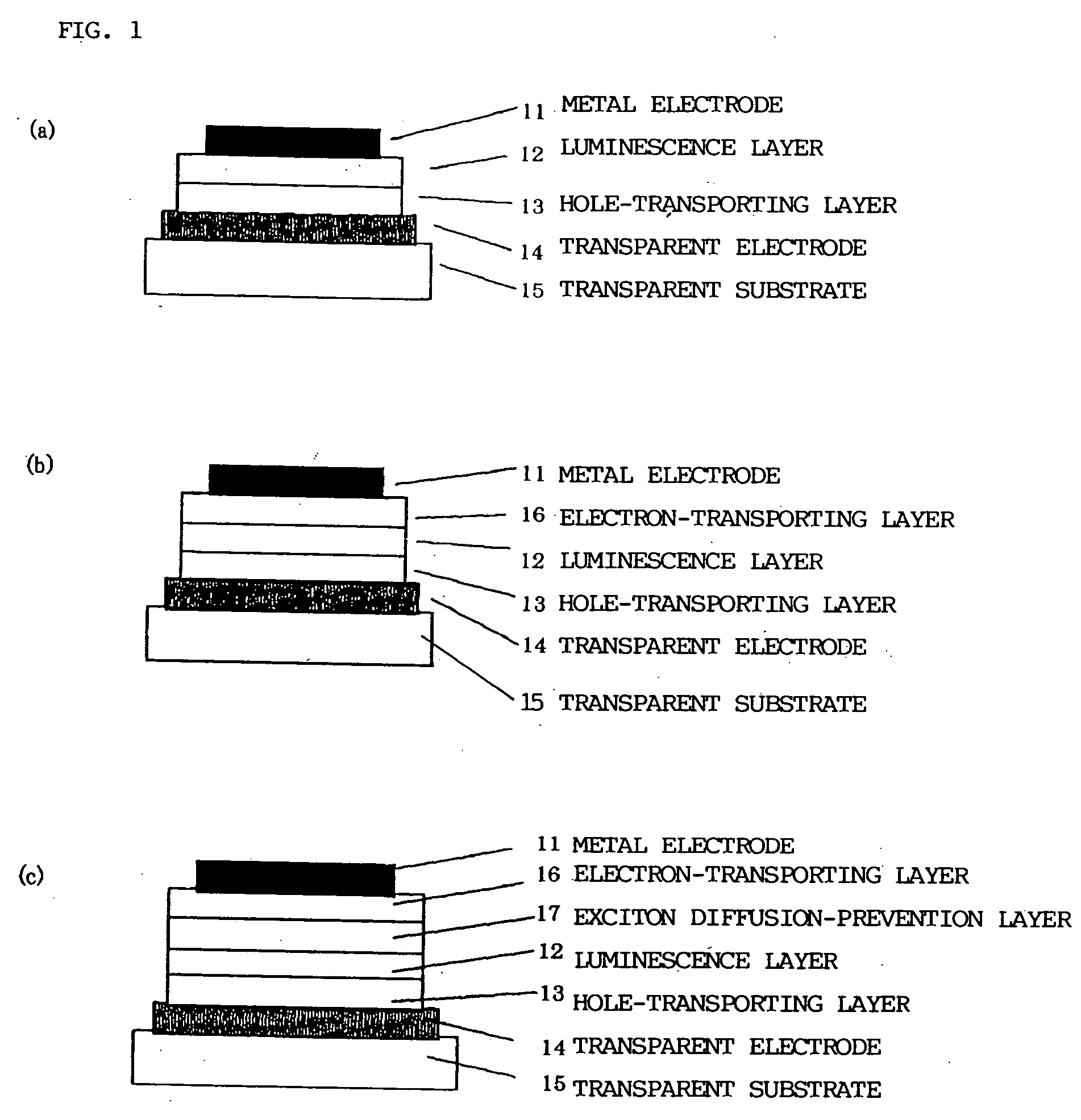
[0183] In these Examples, a device (effective display area=3 mm2) having a device structure including 4 organic layers as shown in FIG. 1(c) was prepared. An alkali-free glass sheet was used as a transparent substrate 15 and a 100 nm-thick indium oxide (ITO) film was formed by sputtering and patterned as a transparent electrode 14. Further, α-NPD represented by the above-mentioned structural formula was vacuum-deposited in a layer thickness of 40 nm thereon as a hole-transporting layer 13. Then, as an organic luminescence layer 12, the above-mentioned CBP as a host material and a prescribed metal coordination compound in an amount of providing 8 wt. % were co-vacuum deposited in a layer thickness of 30 nm. Further, as an exciton diffusion-prevention layer 17, BCP was vacuum-deposited in a thickness of 10 nm. Then, as an electron-transporting layer 16, the above-mentioned Alq3 was subjected to resistance heating vacuum deposition at a vacuum of 10−4 Pa to form an organic film in a th...

example 6

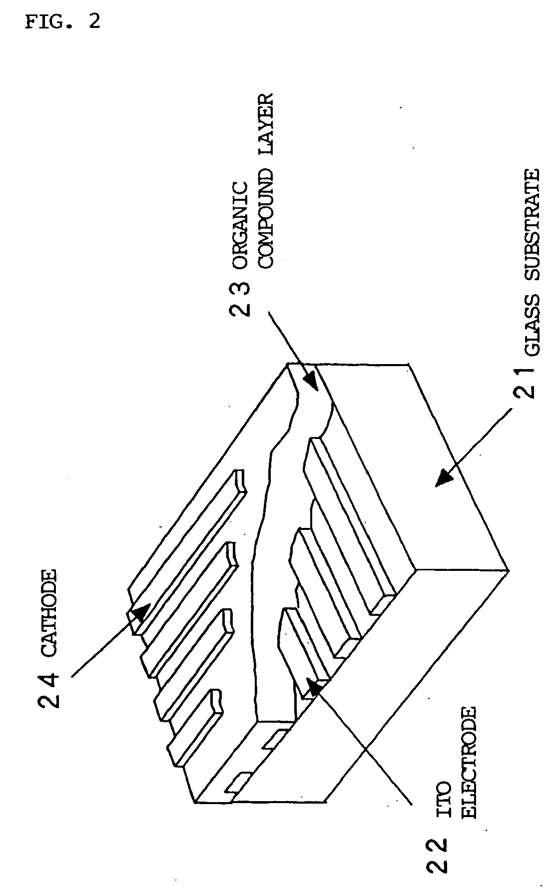
[0194] A simple matrix type organic EL device as shown in FIG. 2 was prepared in the following manner.

[0195] On a glass substrate 21 measuring 100 mm-length, 100 mm-width and 1.1 mm-thickness, a ca. 100 nm-thick ITO film was formed by sputtering and patterned into 100 lines of 100 μm-wide transparent electrodes 22 (anode side) with a spacing of 40 μm as simple matrix electrodes. Then, formed layers of identical organic materials were found under identical conditions as in Example 1 to form an organic compound layer 23.

[0196] Then, 100 lines of 100 μm-wide Al electrodes 24 were formed with a spacing of 40 μm by mask vacuum deposition so as to be perpendicular to the transparent electrodes 22 by vacuum deposition at a vacuum of 2.7×10⁻³ Pa. The metal electrodes (cathode) 24 were formed as a lamination of 10 nm-thick layer of Al / Li alloy (Li: 1.3 wt. %) and then 150 nm-thick layer of Al.

[0197] The thus-obtained 100×100-simple matrix-type organic EL device was subjected to a simple m...


PUM

PropertyMeasurementUnit
luminanceaaaaaaaaaa

Abstract

A luminescence device having a layer containing a metal coordination compound which has a partial structure. MLm of formula (2) below and is preferably entirely represented by formula (3) below: MLmL′n  (3) wherein M denotes a metal atom of Ir, Pt, Rh or Pd; represent mutually different bidentate ligands; m is 1 or 2 or 3; n is 0 or 1 or 2 with the proviso that m+n=2 or 3; the partial structure MLm is represented by formula (2) below (wherein B is an isoquinolyl group bonded to the metal M with its N and including a position-1 carbon atom bonded to a cyclic group A which includes the C bonded to the metal M), and the partial structure ML′n is represented by formula (4), (5) or (6) shown below. There is provided a luminescence device capable of high-efficiency luminescence and long-term high luminance and adapted to red luminescence.

Description

[0001] This application is a division of application Ser. No. 10 / 073,012, filed Feb. 12, 2002, which is a continuation of International Application PCT / JP01 / 10487, filed Nov. 30, 2001. Both prior applications are incorporated herein by reference.TECHNICAL FIELD [0002] The present invention relates to an organic luminescence device (also called an organic electroluminescence device or organic EL device) for use in a planar light source, a planar display, etc. Particularly, the present invention relates to a novel metal coordination compound and a luminescence device having a high luminescence efficiency and causing little change with time by using a metal coordination compound of a specific structure. BACKGROUND ART [0003] An old example of organic luminescence device is, i.e., one using luminescence of a vacuum-deposited anthracene film (Thin Solid Films, 94 (1982) 171). In recent years, however, in view of advantages, such as easiness of providing a large-area device compared with ...

Claims


Application Information

Patent Timeline
Patent Type & Authority Applications(United States)
IPC IPC(8): H01L51/54H05B33/14C09K11/06C07D217/00C07F15/00H01L51/00H01L51/30H01L51/50
CPCC07F15/004H01L51/5234C07F15/008C07F15/0093C09K11/06C09K2211/1007C09K2211/1011C09K2211/1029C09K2211/1033C09K2211/1037C09K2211/1044C09K2211/1048C09K2211/1051C09K2211/1092C09K2211/185H01L51/005H01L51/0059H01L51/0081H01L51/0084H01L51/0085H01L51/5012H01L51/5016H05B33/14Y10S428/917H01L27/3244C07F15/0066H10K85/60H10K85/631H10K85/341H10K85/324H10K85/342H10K50/11H10K2101/10C07F15/00H10K50/828H10K59/12
Inventor KAMATANI, JUNOKADA, SHINJIROTSUBOYAMA, AKIRATAKIGUCHI, TAKAOMIURA, SEISHINOGUCHI, KOJIMORIYAMA, TAKASHIIGAWA, SATOSHIFURUGORI, MANABU
Owner CANON KK
Why Eureka
Try Eureka