Method of forming copper wiring layer

a technology of copper wiring and copper wire, which is applied in the direction of basic electric elements, electrical equipment, and semiconductor devices, etc., can solve the problems of increasing manufacturing costs, increasing the cross-sectional area of wiring, and raising many problems to be solved

Inactive Publication Date: 2006-08-10
TOSHIBA MOBILE DISPLAY CO LTD
View PDF14 Cites 35 Cited by
  • Summary
  • Abstract
  • Description
  • Claims
  • Application Information

AI Technical Summary

Benefits of technology

[0016] It is an object of the present invention to provide a method of forming a copper wiring layer and a method of manufacturin

Problems solved by technology

Therefore, if it is desired to perform the etching of copper by making use of an etching technique such as RIE, the temperature of the substrate is required to be raised to 200 to 300° C. or more, thus raising many problems to be solved before such an etching technique is actually realized.
However, the damascene method disclosed in JP Patent Laid-open Publication (Kokai) No. 2001-189295 (2001) is accompanied with the following problems.
As a result, the manufacturing process involved in this damascene method would become very complicated, resulting in increase in manufacturing cost.
However, because of necessity to enhance the integration of semiconductor elements, there is restriction in any attempt to increase the cross-sectional area of wiring.
However, it is difficult to fill a trench or a via-hole which is narrow in width and large in depth with copper, resulting in insufficient filling of copper.
Further, the step of CMP to polish the copper thin film that has been formed all over the surface of substrate in advance to thereby remove a redundant portion of copper so as to flatten the surface is accompanied with a problem that it takes a long time for accomplishing the treatment, thus degrading the throughput.
Although there has been developed a large-scale CMP device which

Method used


Image

  • Method of forming copper wiring layer
  • Method of forming copper wiring layer
  • Method of forming copper wiring layer

Examples


Embodiment Construction

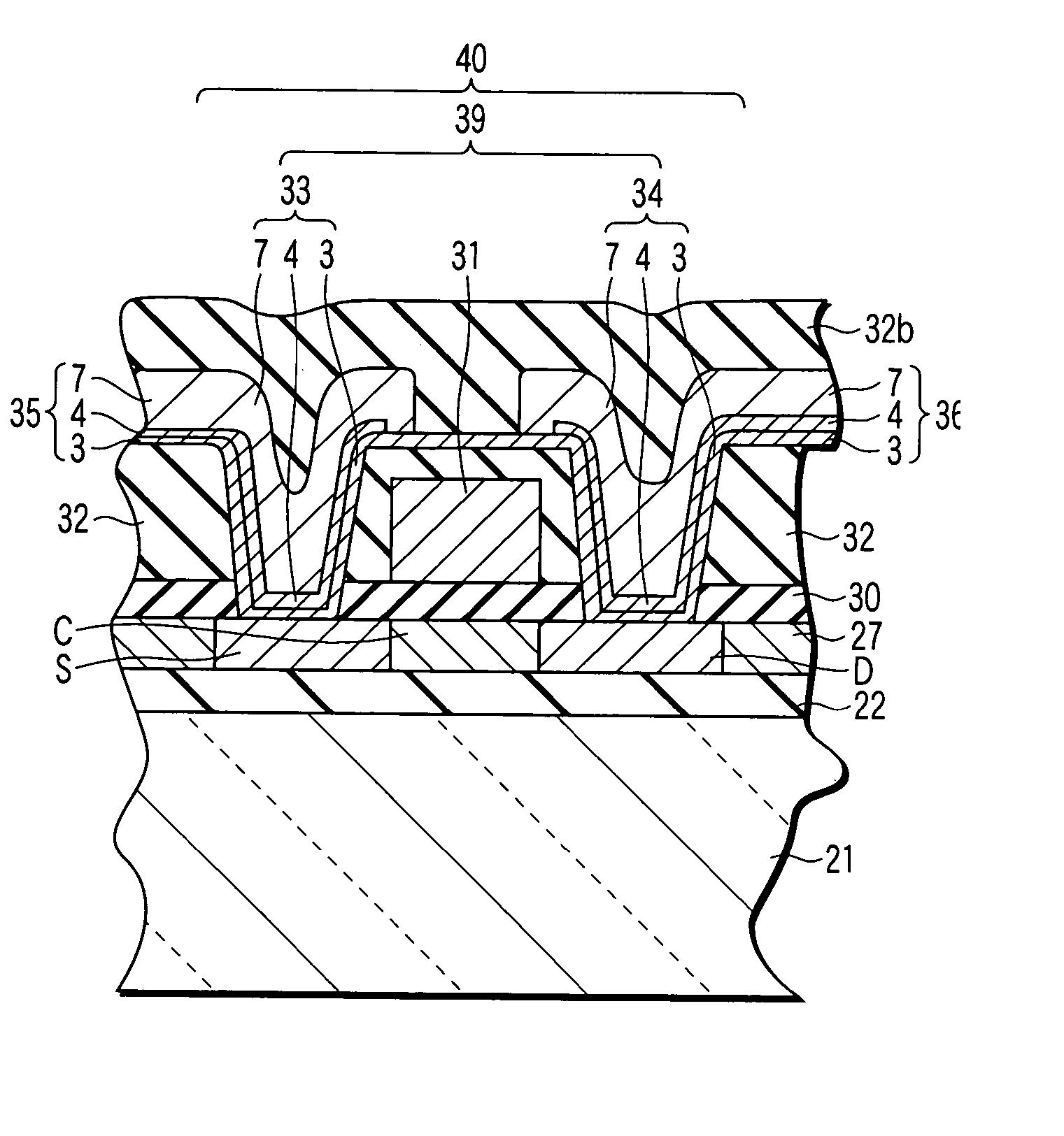
[0031] There is known a method to directly form a copper layer on a barrier layer formed in advance on a substrate by means of electroless plating after forming palladium nuclei on the barrier layer by treatment of palladium catalyst. In this method, however, the copper layer is plated only on the palladium nuclei (several nm to several tens nm). Where the plated copper film is very thin, therefore, it is difficult to form a continuous copper film if it were not to form the palladium nuclei in high density. Therefore, it is difficult to form a plated copper layer having a uniform thickness on a surface of large area.

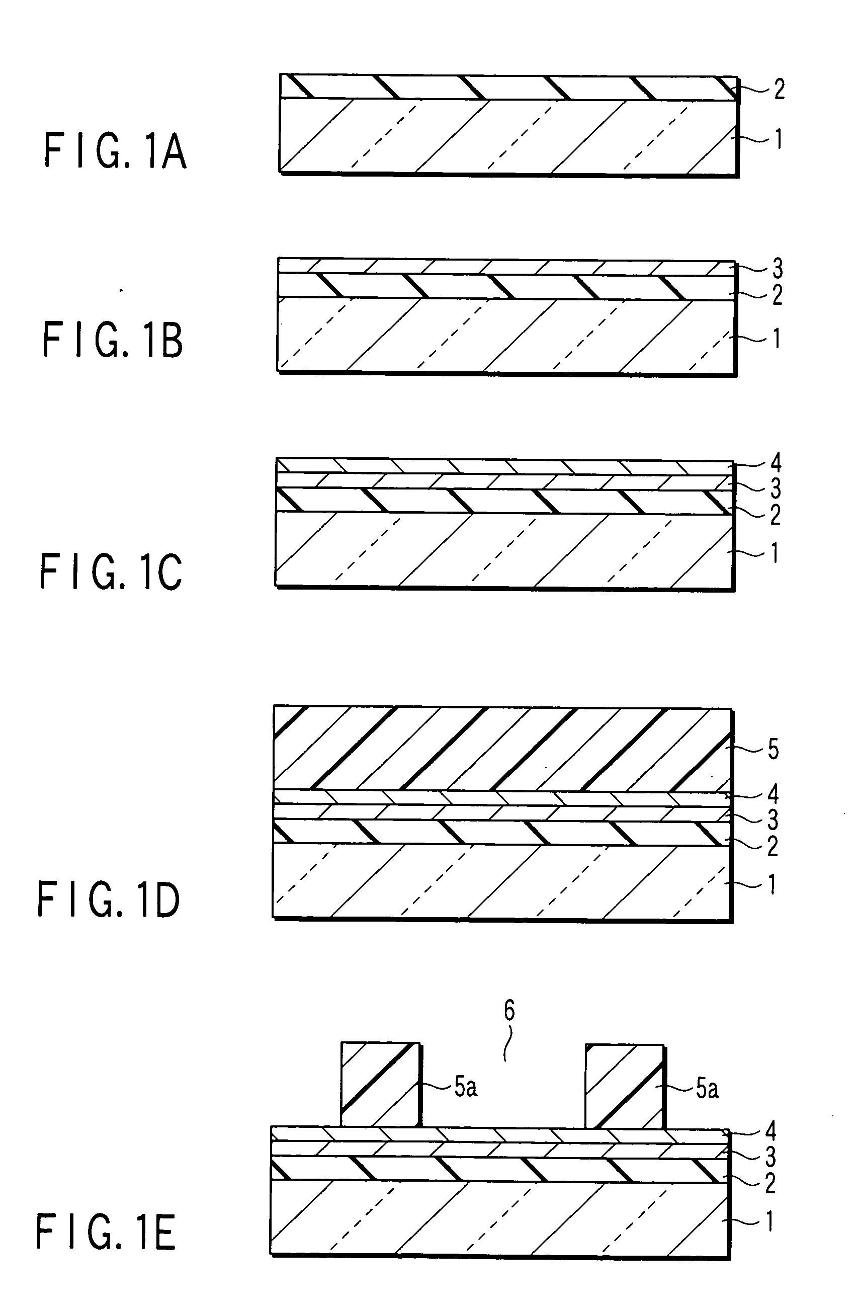
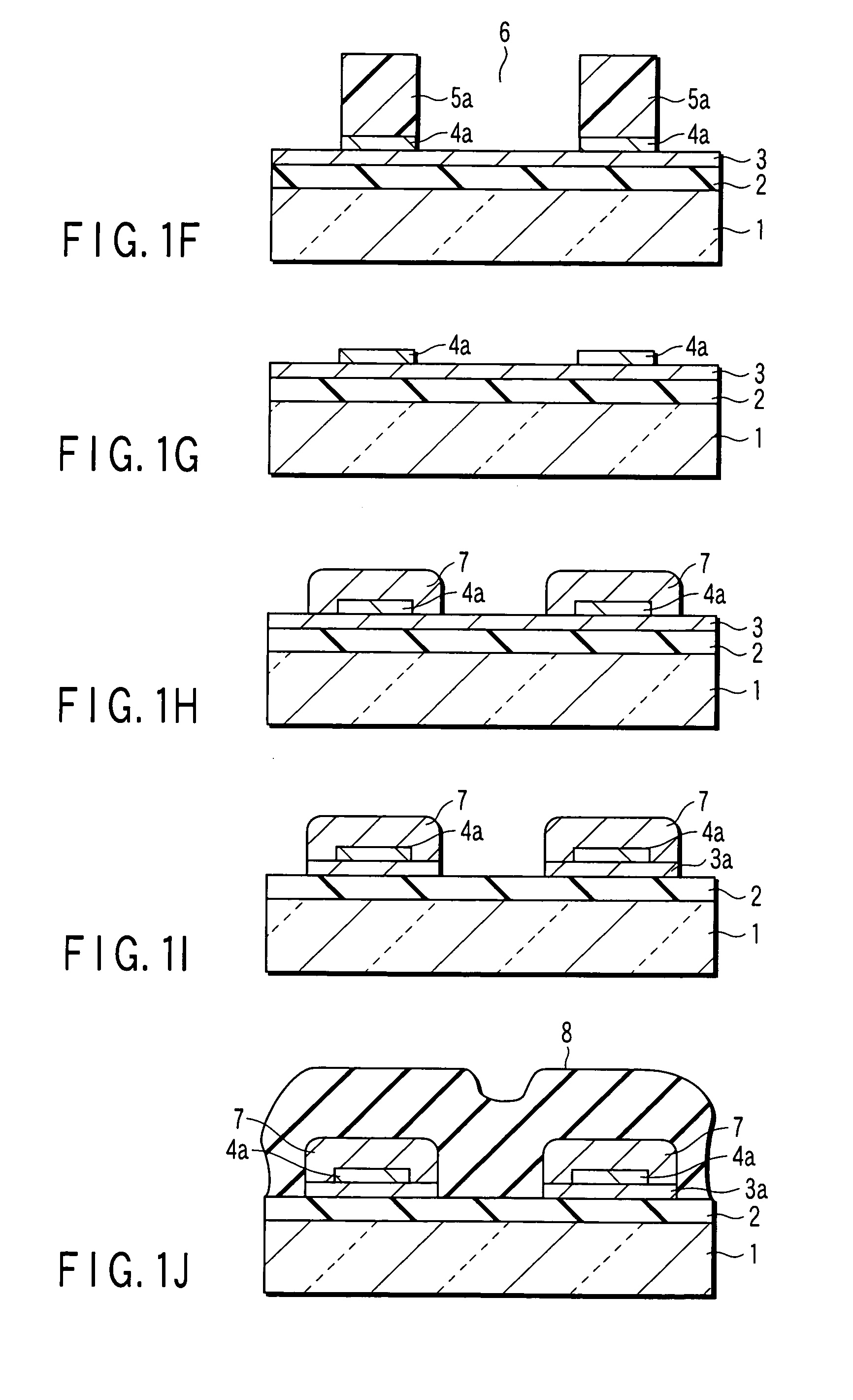
[0032] In the present invention, however, the aforementioned problems are completely dissolved by forming a copper wiring pattern by means of electroless plating on a pattern of a copper seed layer formed in advance on the surface of substrate.

[0033] In this case, the formation of a pattern of copper seed layer is performed by the steps of forming a copper seed layer o...


PUM


Abstract

A method of forming a copper wiring layer, which includes forming a pattern of copper seed layer on a substrate, and forming a copper wiring pattern on the pattern of copper seed layer by means of electroless plating. At least one component of semiconductor device selected from the group consisting of the gate electrode, the source electrode, the drain electrode, and a wiring connected with at least one of these electrodes is formed by a method comprising forming a pattern of copper seed layer, and forming a copper wiring pattern on the pattern of copper seed layer by means of electroless plating.

Description

CROSS-REFERENCE TO RELATED APPLICATIONS [0001] This application is based upon and claims the benefit of priority from prior Japanese Patent Application No. 2005-028919, filed Feb. 4, 2005, the entire contents of which are incorporated herein by reference. BACKGROUND OF THE INVENTION [0002] 1. Field of the Invention [0003] This invention relates to a method of forming a copper wiring layer, which is capable of forming a fine wiring of low resistance, to a method of manufacturing a semiconductor device. In particular, this invention relates to the formation of a copper wiring layer which is suited to the manufacture of a display device represented by a liquid display device as well as for the manufacture of a semiconductor device such as a ULSI. [0004] 2. Description of the Related Art [0005] Generally, aluminum (Al) or alloys thereof are employed as a wiring material in a semiconductor device represented by an LSI and ULSI. However, due to demands for further refinement of the wiring...

Claims


Application Information

Patent Timeline
IPC IPC(8): H01L21/44
CPCH01L21/76843H01L21/76852H01L21/76855H01L21/76864H01L21/76874H01L21/76879H01L21/76885H01L21/76888H01L27/124H01L27/1292H01L27/1296H01L29/458H01L21/28
Inventor NAKAMURA, HIROKIKADO, MASAKIAOMORI, SHIGERU
Owner TOSHIBA MOBILE DISPLAY CO LTD
Why Eureka
Try Eureka