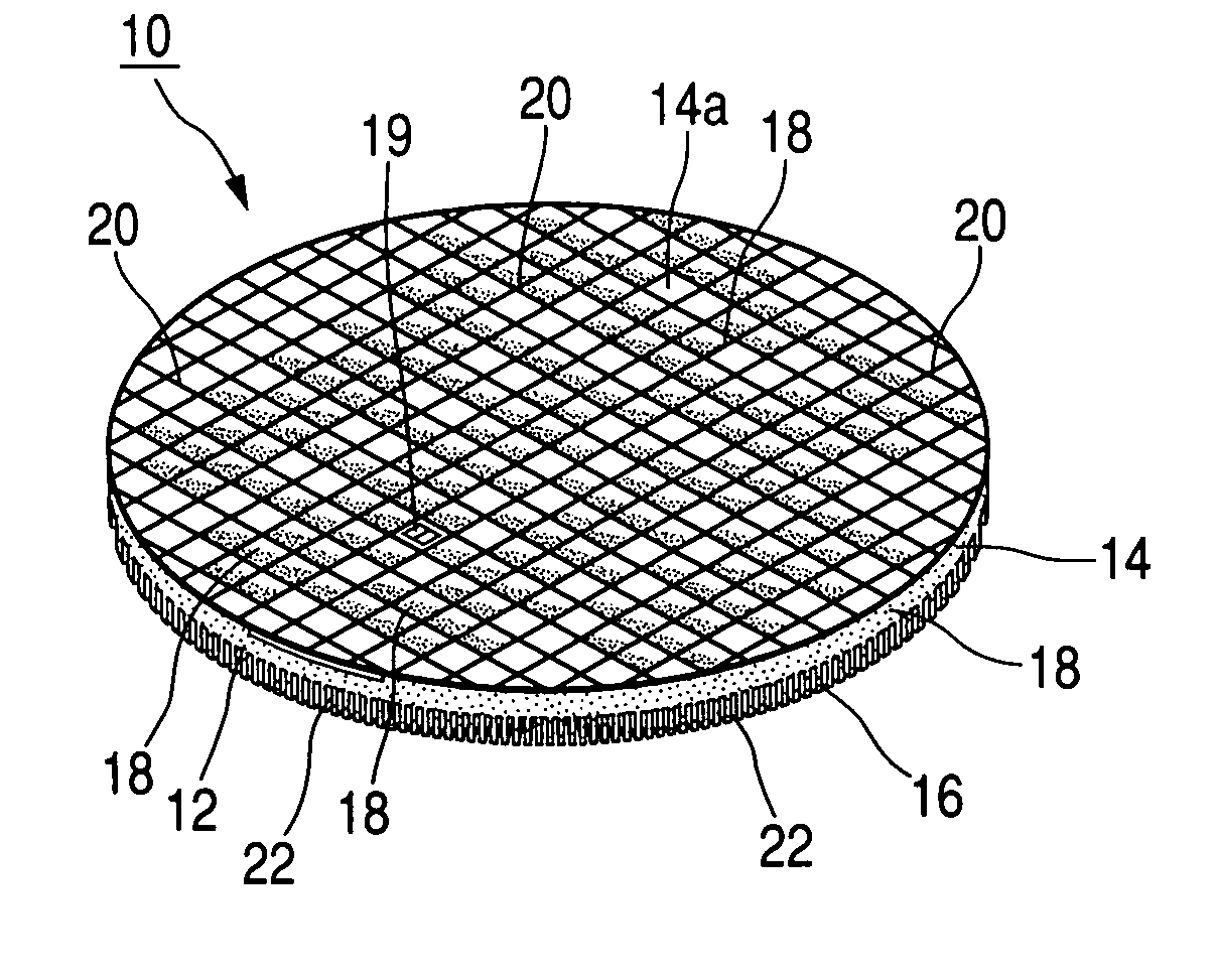
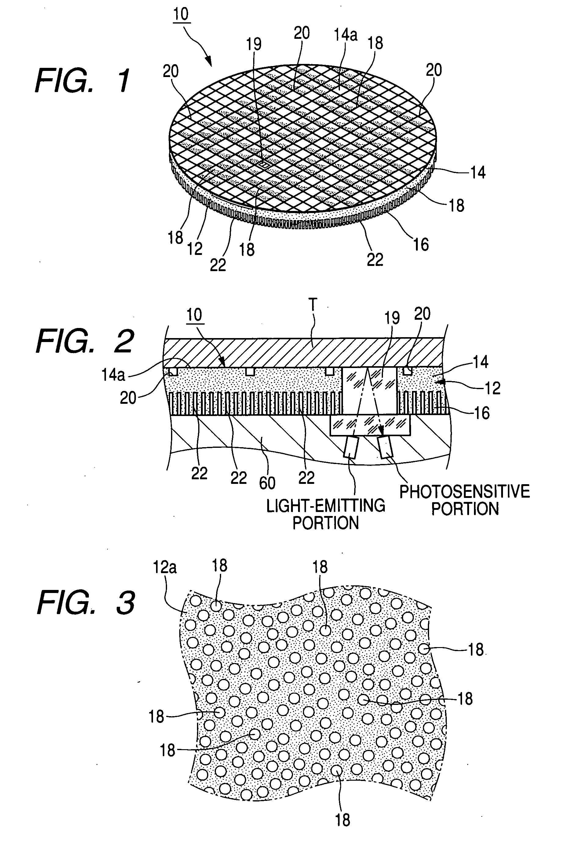
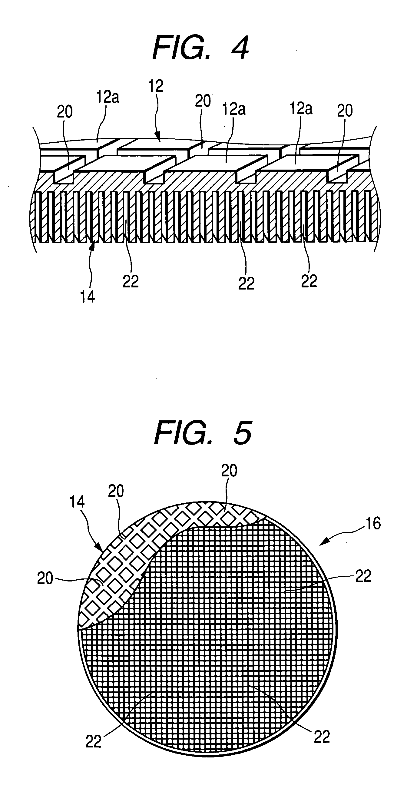
Polishing pad

a technology of polishing pad and rotary plate, which is applied in the direction of grinding/polishing hand tools, metal-working equipment, metal-working equipment, etc., can solve the problems of disordered in-plane uniformity, difficult to achieve high-precision leveling of semi-conductor wafers, and inability to effect sufficient focusing or form fine wiring structures, etc., to achieve excellent step height reduction and in-plane uniformity

Inactive Publication Date: 2006-08-10
INOAC CORP +1
View PDF8 Cites 26 Cited by
  • Summary
  • Abstract
  • Description
  • Claims
  • Application Information

AI Technical Summary

Benefits of technology

[0013] In the light of problems with polishing pads according to the related art, the invention has been proposed to solve fairly these problems. An aim of the invention is to provide a single-layered polishing pad having been integrally molded by reaction injection molding, which is suitable for chemical mechanical polishing (CMP) of a semi-conductor wafer, etc. and which can attain excellent step height reduction and in-plane uniformity.

Problems solved by technology

In the process for forming a multi level interconnection, when there is a certain or higher difference in height of concave and convex in the interlayer dielectrics or metal wirings, it is made impossible to effect sufficient focusing or form a fine wiring structure.
The high precision leveling of a semi-conductor wafer can be difficultly attained by conventional SOG (spin on glass) or etching.
On the other hand, however, since follow-up properties to waviness and mild concave and convex (generally called “nanotopography”) of the surface of the object to be polished are low, the in-plane uniformity is disordered.
That is, it was difficult to cope with both the step height reduction (1) and the in-plane uniformity (2).
In the problem (1), the in-plane uniformity on the surface of the resulting object to be polished cannot be kept.
Accordingly, it cannot be observed from the outside, and the discovery is difficult (actually, the discovery of the air accumulation is judged only from the results regarding the polishing state on the surface of the object to be polished such as wafers).
Also, since these problems cannot be surely avoided without skill of the sticking works, it is difficult to prevent such problems from occurring.
If a part of the stress reduction layer 54 is stretched in the horizontal direction, different flexibility is revealed depending upon the site of the stress reduction layer 54, resulting in making it impossible to attain sufficient in-plane uniformity.
In this case, however, the lamination at the time of production is difficult, and the deterioration of the production yield leads to an increase of the production cost.
Accordingly, this method could not be a fundamental dissolution method.

Method used


Image

  • Polishing pad
  • Polishing pad
  • Polishing pad

Examples


experiment 1

(Results of Experiment 1)

[0092] The results of the various measurement items are shown in Table 1. It has been confirmed from Table 1 that when the amount of deflection of the resulting polishing pad is 15 μm or more, both good step height reduction and in-plane uniformity are revealed. Further, it has been confirmed that when the stress reduction region is 2.0 mm as the upper limit, the necessary density is not more than 0.35 g / cm3.

TABLE 1Various physical property valuesPolishingAcharacteristicsBulk density (g / cm3)CDStressAmount ofStepEFPolishingreductionBdeflectionheightIn-planeOverallregionregionD hardness(μm)reductionuniformityevaluationExample 10.730.155536GGGExample 20.730.355515GGGComparative0.730.405514GPPExample 1Comparative0.730.505511GPPExample 2

(Experiment 2)

Re: Relationship Between Thickness and Amount of Deflection in Stress Reduction Region

[0093] Basically, a conventionally known polishing pad having a multilayered structure (trade name: IC-1400, manufactured by...

example 3

[0095] Single-layered polishing pad having a depth of the stress reduction portion (thickness of the stress reduction region) of 0.80 mm and a thickness of the polishing region of 1.70 mm

example 4

[0096] Single-layered polishing pad having a depth of the stress reduction portion (thickness of the stress reduction region) of 1.23 mm and a thickness of the polishing region of 1.27 mm


PUM

PropertyMeasurementUnit
densityaaaaaaaaaa
sizeaaaaaaaaaa
step heightaaaaaaaaaa

Abstract

A single-layered polishing pad suitable for chemical mechanical polishing (CMP) of semiconductor wafers, etc., which attains excellent step height reduction and in-plane uniformity and is integrally molded by reaction injection molding, is provided. The polishing pad is a polyurethane-based foam 12 having a desired shape, as obtained by molding a gas-dissolved raw material having an inert gas dissolved under pressure in a polyurethane-base resin raw material by a reaction injection molding method, and includes a polishing region 14 having a polishing surface 14a suitable for polishing semi-conductor materials, etc. and having a Shore D hardness in the range of from 40 to 80 and a stress reduction region 16 which is present in the side opposing to the polishing surface 14a and which, when provided with a stress adjusting portion 22 of a desired pattern, is set up so as to have an amount of deflection, as applied with a load of 0.05 MPa, of 10 μm or more.

Description

FIELD OF THE INVENTION [0001] The present invention relates to a polishing pad and more particularly to a polishing pad having a polishing region and a stress reduction region integrally molded therewith, which can effectively polish an object to be polished having high requirements for precision and surface flatness, such as semi-conductor wafers, by chemical mechanical polishing (CMP). BACKGROUND OF THE INVENTION [0002] One of important technologies supporting the recent rapid technical progress is the development of equipment of information technology such as computers. It is not too much to say that the development of performance of the aforementioned information technology can be attained by the development of performance and / or integration of CPU (central processing unit) of information engineering equipment, i.e., ULSI (ultra large scale integrated) devices constituting CPU. As one of methods for drastically developing the performance and / or integration of ULSI devices, a met...

Claims


Application Information

Patent Timeline
Patent Type & Authority Applications(United States)
IPC IPC(8): B24D17/00B24D99/00
CPCB24B37/205B24B37/24B24B37/26
Inventor HISHIKI, SEIGO
Owner INOAC CORP
Why Eureka
Try Eureka