Data communication method and apparatus utilizing programmable channels for allocation of buffer space and transaction control

a data communication and buffer space technology, applied in the field of digital data processing hardware, can solve the problems of increasing the complexity of the modern computer system, the cost of capability, and the complexity of the digital computer system itself, and achieve the effect of being ready to adapt to the connection

Inactive Publication Date: 2006-08-10
IBM CORP
View PDF18 Cites 51 Cited by
  • Summary
  • Abstract
  • Description
  • Claims
  • Application Information

AI Technical Summary

Benefits of technology

[0025] In the preferred embodiment, the integrated circuit chip is a bridge chip for coupling multiple data buses of a computer system. The functional modules within the chip are data bus interface modules for interfacing with the data buses, the data buses being external to the integrated circuit chip. The use of different functional modules coupled by the central interconnect enables the chip to support communications between buses of different types.
[0029] The use of a flow control mechanism in which transactions are assigned to channels having programmable attributes, each channel having independent flow control, provides a flexible flow control mechanism which can be configured efficiently for a variety of system environments. This flexible flow control mechanism is particularly suitable for use in an internal central interconnect and internal buses of an ASIC. This internal chip communications architecture is readily adaptable to connect with functional components of different types, therefore supporting a variety of different specific ASIC designs.

Problems solved by technology

A modern computer system is an enormously complex machine, usually having many sub-parts or subsystems, each of which may be concurrently performing different functions in a cooperative, although partially autonomous, manner.
Each component of a digital computer system is itself a very complex instrument, having a design hierarchy which can mimic that of the system.
Unfortunately, this capability comes at a cost.
All of these operations take time.
Additionally, because the CPU is doing so many things at a time, it typically consumes a relatively large amount of power.
Such smaller, special-purpose digital logic circuits often consume less power than a typical CPU, and because they perform a more limited set of functions, often do so faster than a typical CPU.
It is simply more limited in the variety of functions it can perform.
Many ASICs are programmable to alter their functions within some design range, but in general they do not have the flexibility of a general-purpose CPU.
One of the challenge of using ASICs is the design effort involved.
Although the design of a single ASIC is no more difficult (and often less so) than that of a general-purpose processor, the number of different applications and consequent number of separate ASIC designs can involve a substantial burden in the design and development of a digital system using ASICs.
However, such special circuitry is likely to be different for each permutation of sender and receiver component module, depending on the requirements of the individual components.
For example, it is known to use a “central interconnect” module for handling communications among multiple chip components using a generic interface, but fixed generic interfaces are likely to involve greater overhead and be less than optimal.
Conventional flow control mechanisms, including control of passing, generally limit flexibility and performance optimization.

Method used


Image

  • Data communication method and apparatus utilizing programmable channels for allocation of buffer space and transaction control
  • Data communication method and apparatus utilizing programmable channels for allocation of buffer space and transaction control
  • Data communication method and apparatus utilizing programmable channels for allocation of buffer space and transaction control

Examples


Embodiment Construction

Digital Data Processing Environment

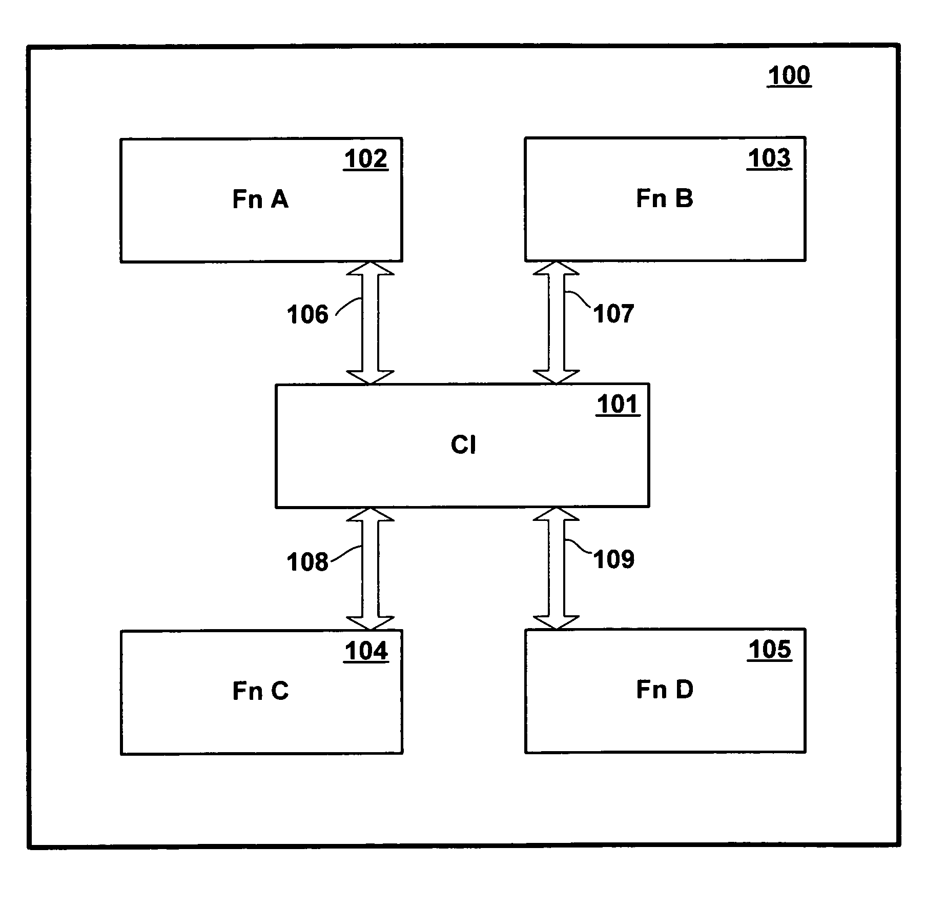
[0045] The present invention relates to the design of digital communications interfaces. In the preferred embodiments, a modular architecture is employed in the design of an integrated circuit chip, whereby a central interconnect module within a chip facilitates data transfer among multiple functional component modules of the chip. Using this architecture, it is possible to design a family of different application specific integrated circuits (ASICs) performing diverse functions, all of which employ a similar central interconnect module design for facilitating internal data transfer. In the exemplary embodiments of the invention described herein, an ASIC performs the function of an I / O bridge interface between different buses of a general-purpose computer system. However, this is but one of many possible implementations and digital data environments in which the present invention might be employed.

[0046] Referring to the Drawing, wherein like nu...


PUM


Abstract

A control mechanism for data bus communications employs channels to which bus transactions are assigned, each channel having independent flow control. The control mechanism enforces an ordering algorithm among channels, whereby at least some transactions may pass other transactions. Channel attributes are programmable to vary the ordering conditions. Preferably, each channel is allocated its own programmable buffer area. The control mechanism independently determines, for each channel, whether buffer space is available and enforces flow control independently for each channel accordingly. Flow control is preferably credit-based, credits representing buffer space or some other capacity of a receiver to receive data. Preferably, the flow control mechanism comprises a central interconnect module controlling internal communications of an integrated circuit chip.

Description

CROSS REFERENCE TO RELATED APPLICATIONS [0001] The present application is related to the following commonly assigned copending applications filed on the same date as the present application, all of which are incorporated by reference: [0002] Application Ser. No. ______, entitled “Internal Data Bus Interconnection Mechanism Utilizing Shared Buffers Supporting Communication Among Multiple Functional Components of an Integrated Circuit Chip” (Assignee's docket number ROC920040239US1); [0003] Application Ser. No. ______, entitled “Internal Data Bus Interconnection Mechanism Utilizing Central Interconnection Module Converting Data in Different Alignment Domains” (Assignee's docket number ROC920040240US1); and [0004] Application Ser. No. ______, entitled “Data Communication Method and Apparatus Utilizing Credit-Based Data Transfer Protocol and Credit Loss Detection Mechanism” (Assignee's docket number ROC920040281US1).FIELD OF THE INVENTION [0005] The present invention relates to digital ...

Claims


Application Information

Patent Timeline
Patent Type & Authority Applications(United States)
IPC IPC(8): G06F3/00
CPCG06F13/4059
Inventor CHADHA, SUNDEEPCHECK, MARK ANTHONYDRERUP, BERNARD CHARLESGRASSI, MICHAEL
Owner IBM CORP
Why Eureka
Try Eureka