Semiconductor device and a method of manufacturing the same

a technology of semiconductors and devices, applied in semiconductor/solid-state device manufacturing, basic electric elements, electric devices, etc., can solve the problems of reducing deteriorating the tddb life, and more difficulty in securing the tddb life, so as to improve the dielectric breakdown strength and reduce the interconnect capacitance

Inactive Publication Date: 2006-08-17
NOGUCHI JUNJI +1
View PDF22 Cites 33 Cited by
  • Summary
  • Abstract
  • Description
  • Claims
  • Application Information

AI Technical Summary

Benefits of technology

[0008] An object of the present invention is to provide a semiconductor device capable of improving the dielectric breakdown strength between interconnects having copper as a main conductor layer, and a method of manufacturing the same.
[0009] Another object of the present invention is to provide a semiconductor device capable of reducing the interconnect capacitance having copper as a main conductor layer, and a method of manufacturing the same.

Problems solved by technology

Since the low dielectric constant insulating film is generally low also in dielectric breakdown strength, there is still more difficulty in securing the TDDB life.
A deterioration in the TDDB life is presumed to occur because diffusion of copper used as an interconnect material lower the dielectric breakdown strength between interconnects.
In addition, the air gap is formed by forming the interconnect to have a reverse taper shape so that the electric field concentrates on the upper end portion of the interconnect, thereby causing a further reduction in the TDDB life.

Method used


Image

  • Semiconductor device and a method of manufacturing the same
  • Semiconductor device and a method of manufacturing the same
  • Semiconductor device and a method of manufacturing the same

Examples


embodiment 1

(Embodiment 1)

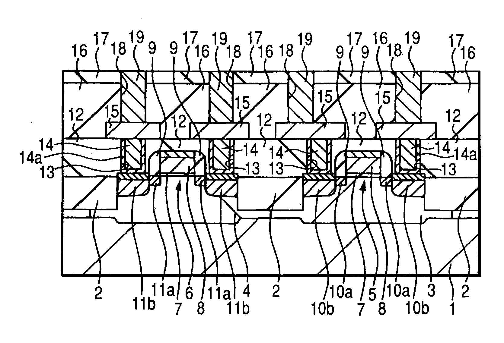
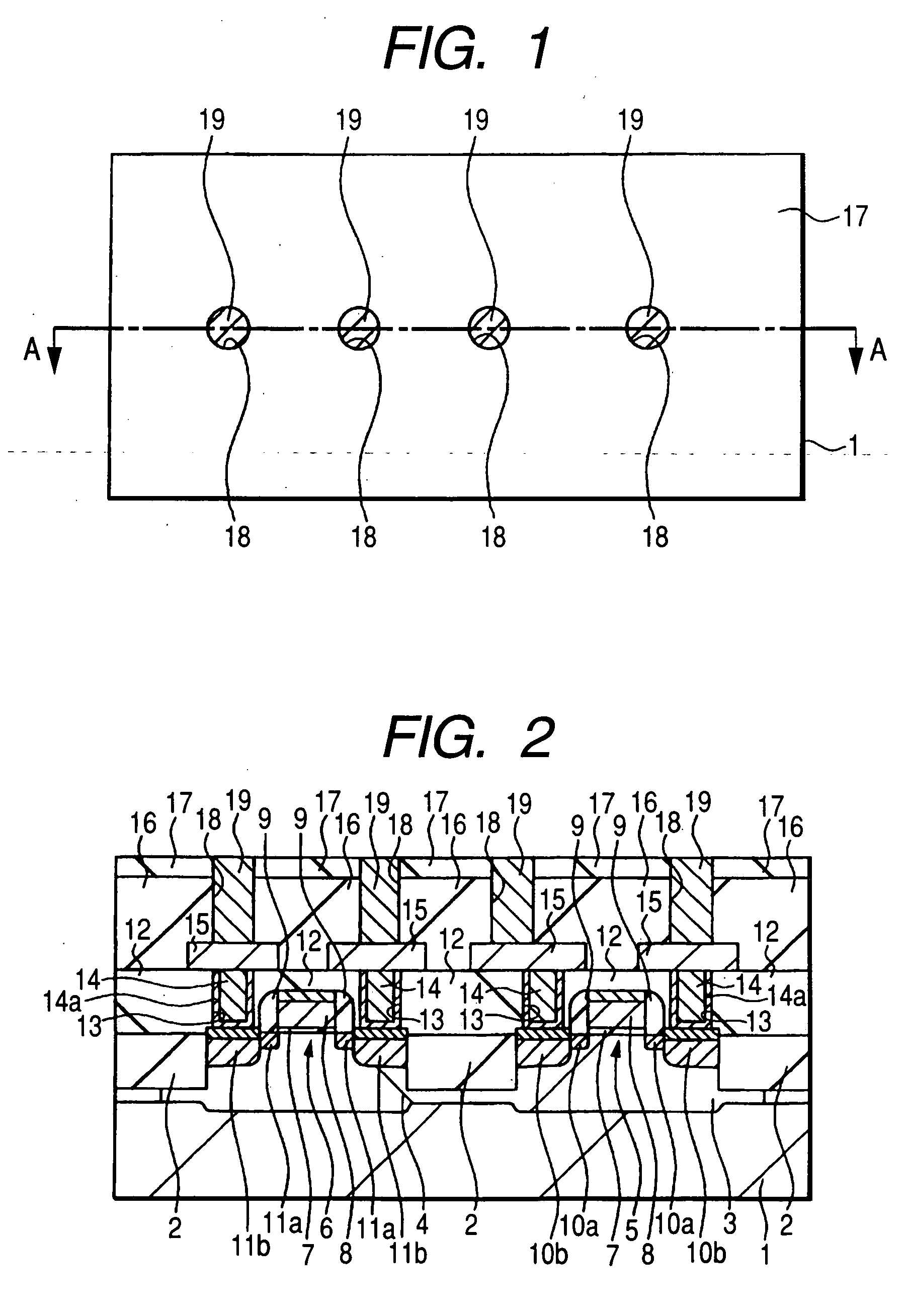
[0051] First, a causes for deteriorating the TDDB life between the inlaid interconnects each having copper as a main conductor layer, which have been investigated by the present inventors, will be described. The term “TDDB (Time Dependence on Dielectric Breakdown) life” is a measure for objectively measuring time-dependence of dielectric breakdown and means time (life) determined by extrapolation to an electric field intensity in actual use (e.g. 0.2 MV / cm) from a graph prepared by applying a comparatively high voltage to between electrodes under a measuring condition at a predetermined temperature (e.g. 140° C.) to plot a time from voltage application up to dielectric breakdown against an applied electric field.

[0052] A deterioration in the TDDB life is presumed to occur because copper employed as an interconnect material diffuses around and lowers dielectric breakdown strength between interconnects. Investigation results by the present inventors however suggest that...

embodiment 2

(Embodiment 2)

[0112] FIGS. 20 to 25 are fragmentary cross-sectional views of the semiconductor device according to another embodiment of the present invention during its manufacturing steps. Manufacturing steps up to FIG. 10 are similar to those of Embodiment 1 so that a description on them is omitted and manufacturing steps following those of FIG. 10 will next be described.

[0113] After formation of the structure as illustrated in FIG. 10, an insulating film 29 made of, for example, a silicon nitride film, and an insulating film 30 made of, for example, a silicon oxide film are formed in this order over the insulating film 28 as illustrated in FIG. 20. CMP treatment is conducted if necessary to planarize the upper surface of the insulating film 30. It is not always necessary to form the insulating film 30.

[0114] Over the insulating film 33, an antireflective film 50a and a photoresist film are formed in this order, followed by patterning of the photoresist film by exposure, whereb...

embodiment 3

(Embodiment 3)

[0123]FIG. 26 is a fragmentary cross-sectional view of a semiconductor device according to a further embodiment of the present invention during its manufacturing step. The semiconductor device according to this embodiment has a multilevel interconnect structure having, in combination, an interconnect layer in which a void is formed between two adjacent interconnects and moreover, two adjacent interconnects are not connected via a CMP surface as the second-level interconnects 25 or third-level interconnects 36 of Embodiment 1; and an interconnect layer formed by the conventional inlaid interconnect forming technique. In FIG. 26, the manufacturing steps up to the formation step of the insulating film 42 are similar to those illustrated in the drawings up to FIG. 19 in Embodiment 1 so that overlapping description is omitted. The manufacturing steps thereafter will next be described.

[0124] In this Embodiment, an insulating film 60 made of silicon oxide is formed over the ...


PUM


Abstract

Provided are a semiconductor device comprising a semiconductor substrate, a first insulating film formed thereover, interconnects formed over the first insulating film and having copper as a main component, a second insulating film formed over the upper surface and side surfaces of each of the interconnects and over the first insulating film and having a function of suppressing or preventing copper diffusion, and a third insulating film formed over the second insulating film and having a dielectric constant lower than that of the second insulating film; and a method of manufacturing the semiconductor device. This invention makes it possible to improve dielectric breakdown strength between copper interconnects and reduce capacitance between the copper interconnects.

Description

CROSS-REFERENCE TO RELATED APPLICATIONS [0001] This application is a Continuation of application Ser. No. 10 / 387,504, filed Mar. 14, 2003, the entire disclosures of which are hereby incorporated by reference.BACKGROUND OF THE INVENTION [0002] The present invention relates to a semiconductor device and a method of manufacturing the same, particularly to a technique effective when applied to a semiconductor device having an interconnect containing a main conductor film having copper as a main component. [0003] An inlaid interconnect structure is formed by embedding an interconnect material in an interconnect opening such as groove or recess formed in an insulating film by a metallization fabrication technique called damascene technique (single damascene or dual damascene technique). When a main interconnect material is copper (Cu), however, it tends to be diffused in an insulating film compared with a metal such as aluminum (Al) so that diffusion of copper in an inlaid interconnect in...

Claims


Application Information

Patent Timeline
Patent Type & Authority Applications(United States)
IPC IPC(8): H01L21/4763
CPCH01L21/76801H01L21/7681H01L21/76811H01L21/76813H01L21/7682H01L21/76832H01L21/76834
Inventor NOGUCHI, JUNJIFUJIWARA, TSUYOSHI
Owner NOGUCHI JUNJI
Why Eureka
Try Eureka