
Photonic crystal-based filter for use in an image sensor

a technology of photonic crystals and filters, applied in the field of semiconductor devices, can solve the problems of high number of defective filters

Active Publication Date: 2006-08-24
APTINA IMAGING CORP
View PDF18 Cites 11 Cited by
  • Summary
  • Abstract
  • Description
  • Claims
  • Application Information

AI Technical Summary

Benefits of technology

The photonic crystal filter provides a simpler and more efficient method for wavelength selection, reducing defects and enabling greater design flexibility in image sensors, while maintaining high optical efficiency and resolution.

Problems solved by technology

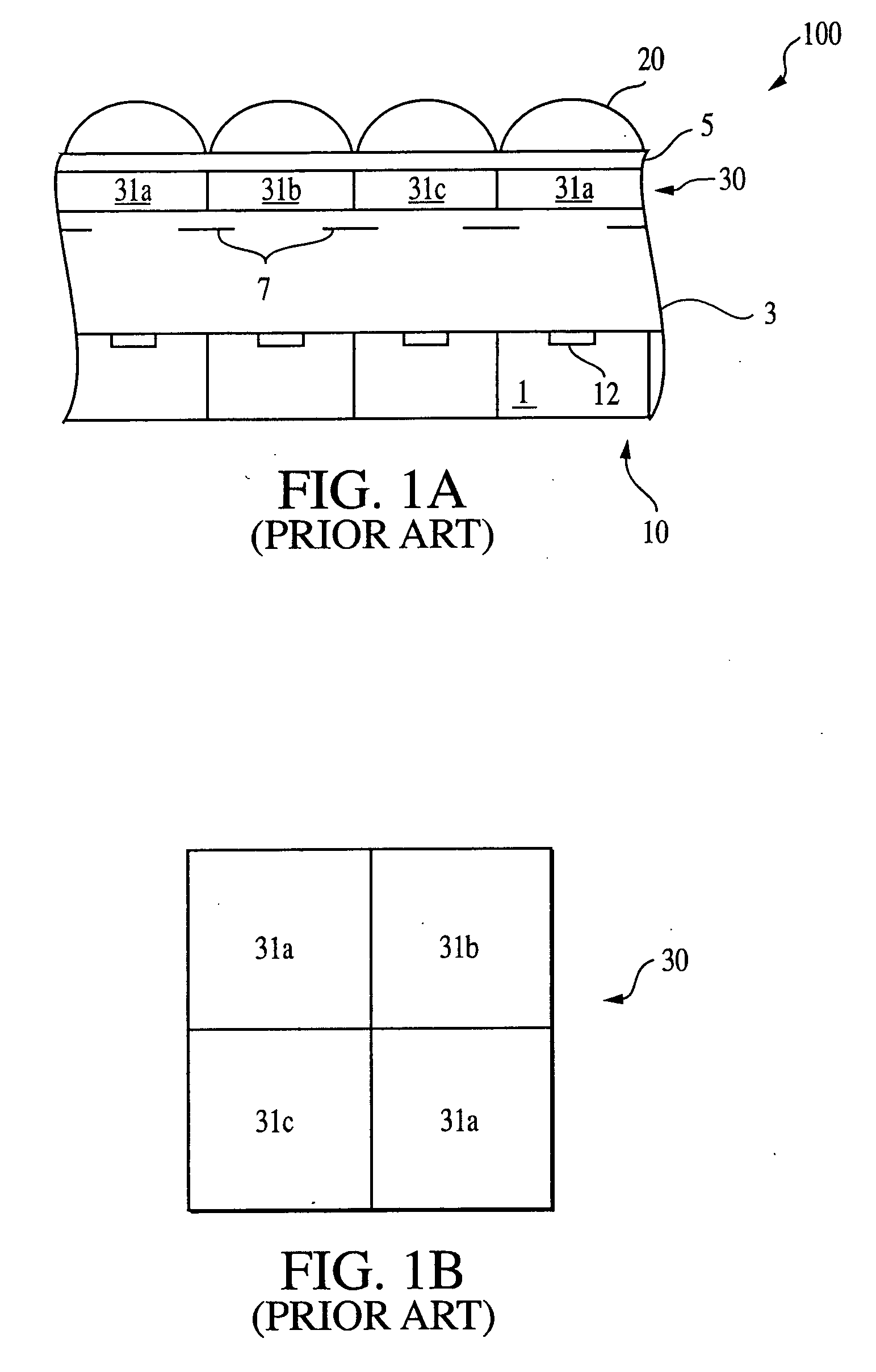
Although color filters prepared using photolithography can exhibit good resolution and color quality, photolithography can be complicated and results in a high number of defective filters 31a, 31b, 31c.

Method used


Image

  • Photonic crystal-based filter for use in an image sensor
  • Photonic crystal-based filter for use in an image sensor
  • Photonic crystal-based filter for use in an image sensor

Examples


Embodiment Construction

[0022] In the following detailed description, reference is made to the accompanying drawings, which form a part hereof and illustrate specific embodiments in which the invention may be practiced. In the drawings, like reference numerals describe substantially similar components throughout the several views. These embodiments are described in sufficient detail to enable those skilled in the art to practice the invention, and it is to be understood that other embodiments may be utilized, and that structural, logical and electrical changes may be made without departing from the spirit and scope of the present invention.

[0023] The terms “wafer” and “substrate” are to be understood as including silicon, silicon-on-insulator (SOI), or silicon-on-sapphire (SOS) technology, doped and undoped semiconductors, epitaxial layers of silicon supported by a base semiconductor foundation, and other semiconductor structures. Furthermore, when reference is made to a “wafer” or “substrate” in the follo...


PUM


Abstract

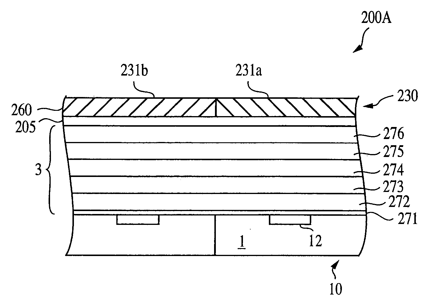
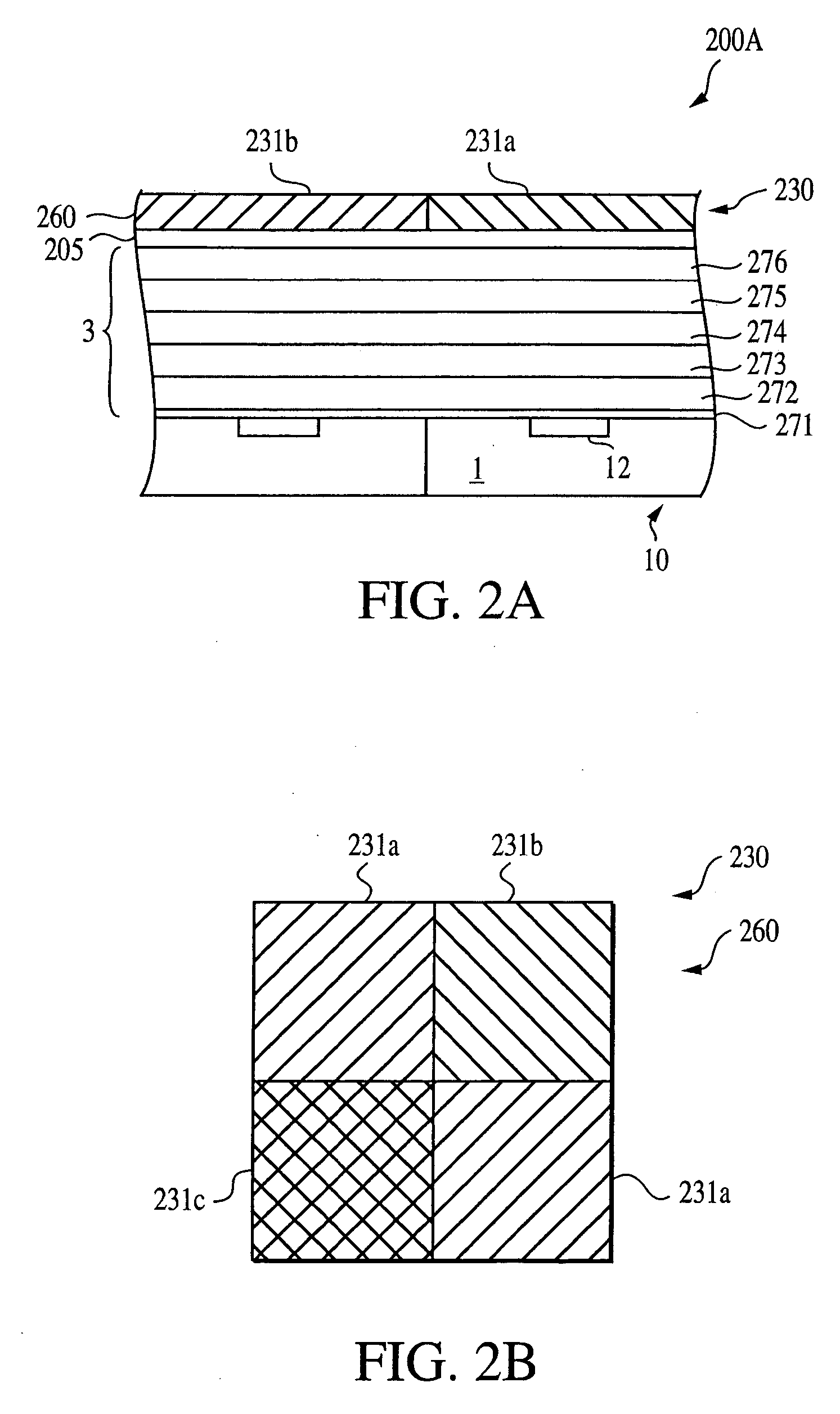
The invention, in various exemplary embodiments, incorporates a photonic crystal filter into an image sensor. The photonic crystal filter comprises a substrate and a plurality of pillars forming a photonic crystal structure over the substrate. The pillars are spaced apart from each other. Each pillar has a height and a horizontal cross sectional shape. A material with a different dielectric constant than the pillars is provided within the spacing between the pillars. The photonic crystal filter is configured to selectively permit particular wavelengths of electromagnetic radiation to pass through.

Description

FIELD OF THE INVENTION [0001] The present invention relates generally to the field of semiconductor devices and more particularly to filters utilized in image sensor devices or displays. BACKGROUND OF THE INVENTION [0002] The semiconductor industry currently uses different types of semiconductor-based image sensors that use micro-lenses, such as charge coupled devices (CCDs), CMOS active pixel sensors (APS), photodiode arrays, charge injection devices and hybrid focal plane arrays, among others. These image sensors use micro-lenses to focus electromagnetic radiation onto the photo-conversion device, e.g., a photodiode. Also, these image sensors can use filters to select particular wavelengths of electromagnetic radiation for sensing by the photo-conversion device. [0003] Micro-lenses of an image sensor help increase optical efficiency and reduce cross talk between pixel cells. FIG. 1A shows a portion of a CMOS image sensor pixel cell array 100. The array 100 includes pixel cells 10,...

Claims


Application Information

Patent Timeline
Patent Type & Authority Applications(United States)
IPC IPC(8): H01L27/00G02B5/20H01L27/146H01L31/0216
CPCG02B5/20H01L27/14621H01L27/14625H01L27/14685H01L31/02165
Inventor MOULI, CHANDRA
Owner APTINA IMAGING CORP
Learn More