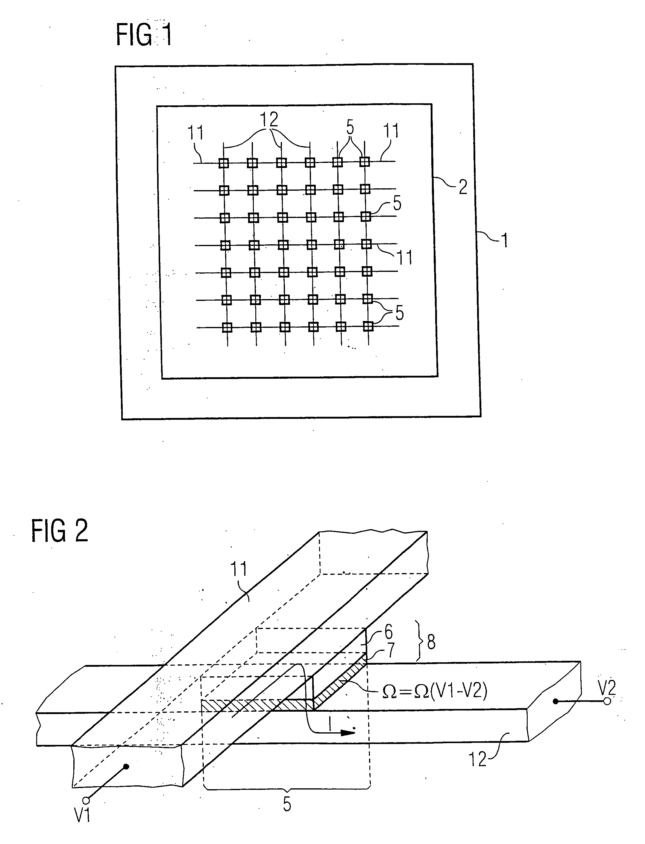
[0016] Embodiments of the invention provide a
semiconductor memory having an arrangement of nonvolatile memory cells, in which the arrangement has a multiplicity of first lines and second lines which can be electrically biased for the purpose of
programming and erasing memory cells. Each memory
cell is coupled to a first line and a second line and has a layer stack that has a
solid electrolyte and that is arranged between the respective first line and the respective second line, to which the memory
cell is coupled. The layer stacks in the memory cells are in a form such that their
ohmic resistance can be altered by the level of a voltage applied between the respective first line and the respective second line and assumes a first value at a sufficiently high positive voltage and a different, second value at a sufficiently high
negative voltage. The first lines and the second lines can be actuated such that electrical potentials on all the first lines and on all the second lines are changed, for the purpose of selectively erasing a selected memory
cell selectively in relation to all the other memory cells in the arrangement of memory cells, such that, respectively, that first line to which the selected memory cell is connected is biased with a first potential selectively in relation to all the other first lines, and that second line to which the selected memory cell is connected can be biased with a second potential selectively in relation to all the other second lines, and all the other first lines are biased with a third potential and all the other second lines are biased with a fourth potential. The
potential difference between the first potential and the second potential is greater than a
limit value for an erasure voltage, above which value any memory cell in the arrangement is reliably erased. The third and the fourth potential are proportioned such that, during the selective erasure of the selected memory cell, voltages applied to the other memory cells are so low that erasure operations and
programming operations in the other memory cells are prevented.
[0018] To prevent the other memory cells connected to the same first line or the same second line as the memory cell which is to be erased from being unintentionally reprogrammed, the invention involves all the other first and second lines also being electrically biased, but with different bias voltages than the selected first and second lines.
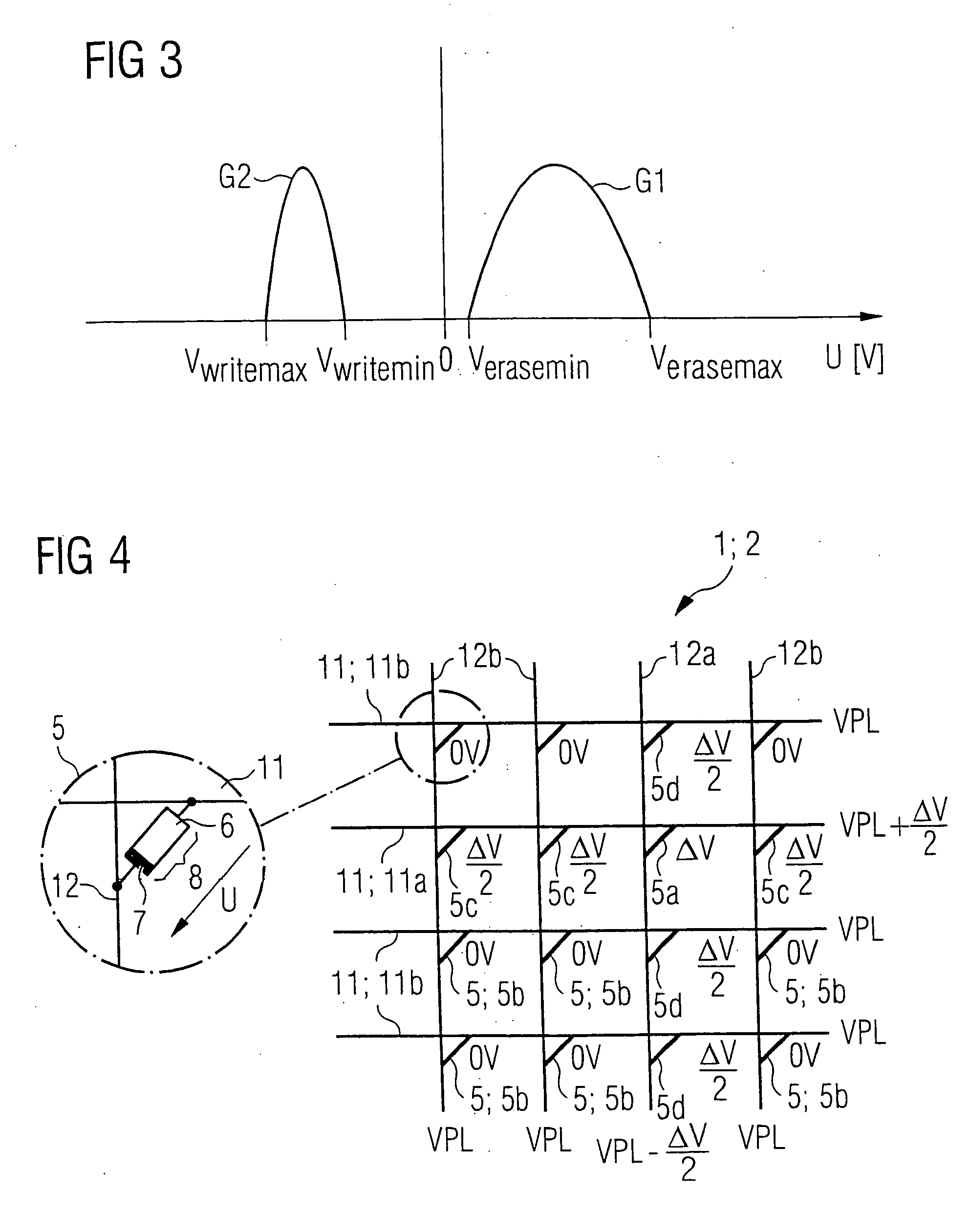
[0024] In the equations disclosed herein, which specify the level of these potentials, VPL is an arbitrary reference potential and Verasemax is a
limit value for an erasure voltage, above which
limit value any memory cell is reliably erased. This limit value is also described below; in FIG. 3, it can be found at the right-hand outer end of the distribution of threshold voltages in the range of positive voltages U for the transition to the high-impedance state. In the equations for the level of the voltages, which are to be applied to the first and second lines, OD denotes a real number, which is at least one, and EI denotes a real number, which is at most one. The magnitude of the parameter OD corresponds to a factor by which the first potential used for erasing the memory cell is excessive in relation to the level of the potential Verasemax. As a result, the erasure operation causes the memory cell to be erased with more certainty and more quickly.
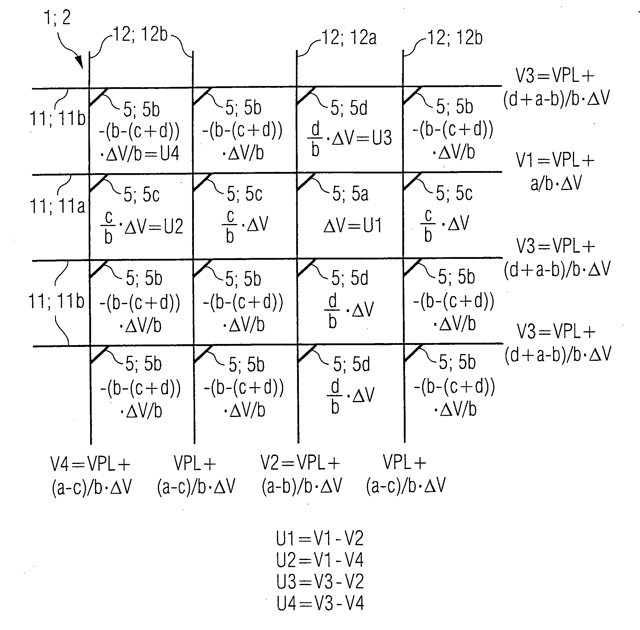
[0032] Preferably, the parameters b, c and d are chosen such that a
negative voltage is applied to those memory cells (5b in FIG. 5) which are connected neither to the first line biased with the first potential nor to the second line biased with the second potential. This embodiment is advantageous because the bandwidth of the threshold values for erasure voltages gets closer to the voltage value 0
volt than the bandwidth of the threshold values for the
programming voltages. For the purpose of selectively erasing a memory cell (the memory cell Sa in FIG. 5), the potential of the first line in question (11a in FIG. 5), to which the memory cell is connected, is raised and the potential of the second line in question (12a in FIG. 5) is lowered. To prevent the other memory cells (5c, 5d in FIG. 5), which are connected to the same first line or the same second line as the selected memory cell (5a in FIG. 5), from likewise being erased, the potential of the other first lines can be lowered and that of the other second lines can be raised. As a result, the other memory cells (5b in FIG. 5) have negative voltages applied to them, whose absolute value needs to be sufficiently small for these memory cells 5b not to be programmed, however. The (negative) voltage applied to these memory cells 5b may be chosen to be smaller (and its absolute value larger) than −Verasemin, i.e., it can assume any value within the range between Vwritemin and Verasemin, said value particularly being able to be between Vwritemin and −Verasemin. This allows for the
asymmetry of the threshold value distributions, which will be explained below with reference to FIG. 3. This means that voltages which are smaller, i.e., negative, but whose absolute value is larger than −Verasemin can be applied to the memory cells 5b. This also allows for the circumstance that Verasemin is smaller for today's solid-electrolyte semiconductor memories than the absolute value of Vwritemin. The
resultant gain in safety is greater the more numerically predominant the number of those memory cells (5b in FIG. 5) which are connected neither to the same first line nor to the same second line as the memory cell which is to be erased, which means that in this embodiment the greatest possible safety against incorrect programming is achieved within the memory cell array.

