Semiconductor device and manufacturing method thereof

a technology of semiconductor devices and semiconductors, applied in semiconductor devices, semiconductor/solid-state device details, electrical apparatus, etc., can solve the problems of difficult entry of molding resin into the gap between the two memory chips, and achieve the effects of improving reliability, high-density packaging, and low cos

Inactive Publication Date: 2006-08-24
RENESAS ELECTRONICS CORP
View PDF10 Cites 13 Cited by
  • Summary
  • Abstract
  • Description
  • Claims
  • Application Information

AI Technical Summary

Benefits of technology

[0011] It is an object of the present invention to provide a technique for improving the reliability and attaining high-density packaging and low cost of a multi-chip module wherein plural chips are mounted on a wiring substrate and a main surface thereof is sealed with resin.
[0012] It is another object of the present invention to provide a technique for improving the reliability of a multi-chip module wherein on plural chips there is stacked another chip and these chips are sealed with resin.
[0013] It is a further object of the present invention to provide a technique capable of reducing the manufacturing cost of a multi-chip module wherein on plural chips there is stacked another chip and these chips are sealed with resin.

Problems solved by technology

In the multi-chip module of the above structure, however, when viewed from the standpoint of high-density packaging, the spacing between the two memory chips arranged side by side is several μm or so and is thus very narrow; besides, the third chip is stacked on those two memory chips, so if an attempt is made to seal these memory chips with a molding resin, there arises the problem that the molding resin is difficult to enter the gap between the two memory chips.

Method used


Image

  • Semiconductor device and manufacturing method thereof
  • Semiconductor device and manufacturing method thereof
  • Semiconductor device and manufacturing method thereof

Examples


first embodiment

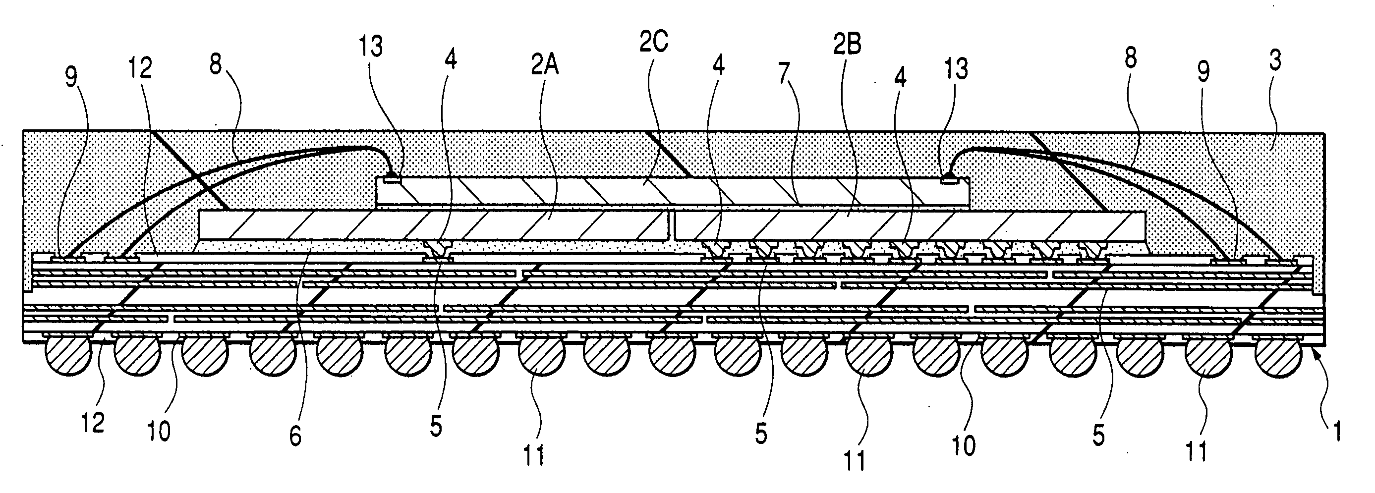
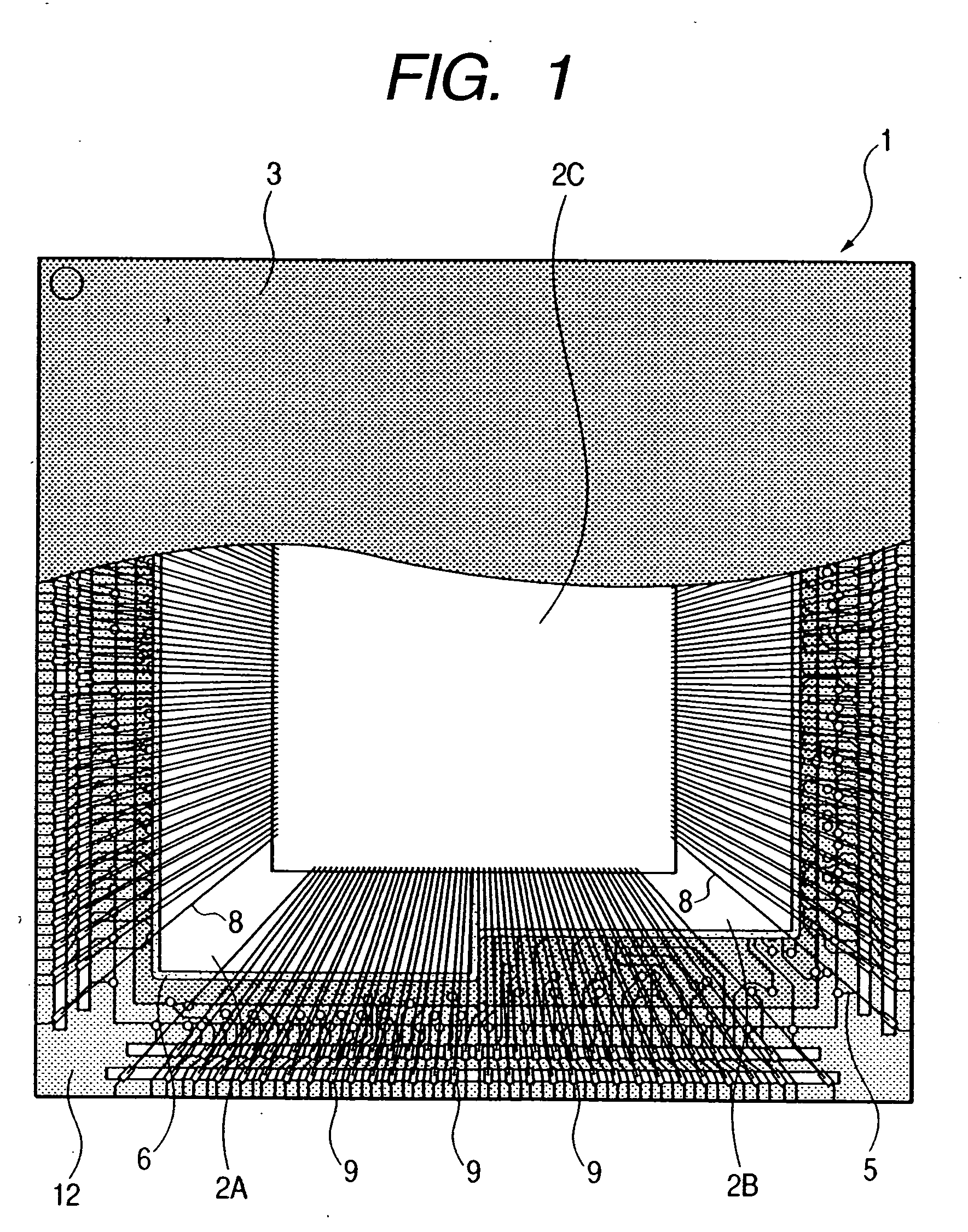
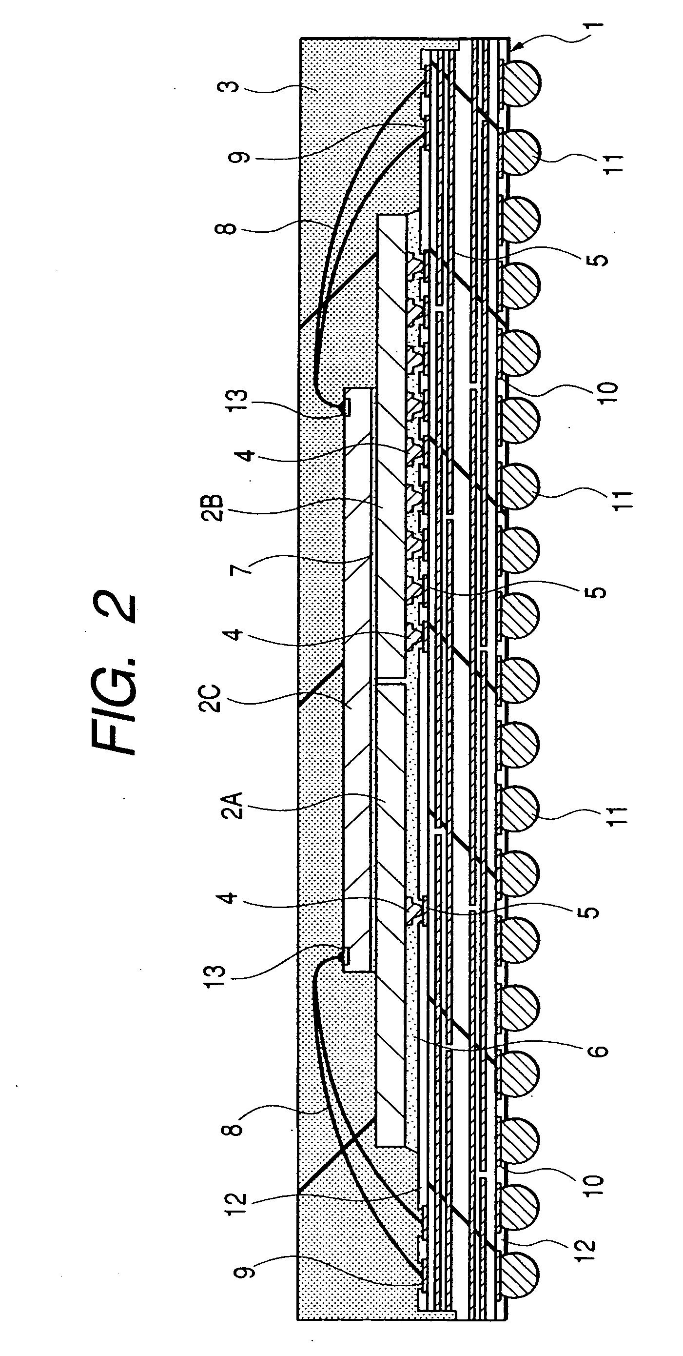
[0071]FIG. 1 is a plan view showing an upper surface of a semiconductor device according to a first embodiment of the present invention, FIG. 1 is a sectional view of the semiconductor device, and FIG. 3 is a plan view showing a lower surface of the semiconductor device.

[0072] The semiconductor device of this embodiment is a multi-chip module (MCM) wherein three chips 2A, 2B and 2C are mounted on a main surface of a package substrate 1 and are sealed with a molding resin 3. Of the three chips 2A to 2C, two chips 2A and 2B are arranged side by side on the main surface of package substrate 1 and are electrically connected to wiring lines 5 on the package substrate 1 through plural Au bumps 4 formed on main surfaces of the chips 2A, 2B. That is, the chips 2A and 2B are each mounted in accordance with a flip-chip method.

[0073] A gap is formed between the main surfaces (lower surfaces) of the chips 2A, 2B and the main surface of the package substrate 1, and an under-fill resin (sealing...

second embodiment

[0100] A method of manufacturing a semiconductor device according to a second embodiment of the present invention will be described below step by step with reference to FIGS. 27 to 34.

[0101] In the previous first embodiment Au bumps 4 are formed on the main surface of the chip 2A with a DRAM formed thereon and also on the main surface of the chip 2B with a flash memory formed thereon, but in this second embodiment there are used solder bumps 20 instead of Au bumps 4.

[0102]FIG. 27 is a plan view showing a state in which solder bumps 20 are formed on a main surface of a chip 2A with a DRAM formed thereon. As shown in the same figure, the solder bumps 20 are arranged in the form of an array on the main surface of the chip 2A. Bonding pads 13 and the solder bumps 20 are electrically connected with each other through Cu wiring lines 21 called re-wiring lines. The Cu wiring lines 21 function as an interposer for converting the pitch of the bonding pads 13 to the pitch of the solder bump...

third embodiment

[0111] A method of manufacturing a semiconductor device according to a third embodiment of the present invention will be described below with reference to FIGS. 35 to 37.

[0112] First, as shown in FIG. 35, solder bumps 20 on chips 2A, 2B and wiring lines 5 on a multi-wiring substrate 100 are electrically connected with each other, then a chip 2C is mounted on the two chips 2A and 2B through an adhesive 7, and thereafter bonding pads 9 on the multi-wiring substrate 100 and bonding pads 13 on the chip 2C are connected together through Au wires 8. These steps are the same as those shown in FIGS. 27 to 31 in the previous second embodiment.

[0113] Then, as shown in FIG. 36, the multi-wiring substrate 100 is loaded into a molding die (not shown) and the whole of a main surface thereof is sealed with resin at a time. At this time, in this embodiment there is used a molding resin 3 with a silica filler added therein, the silica filler having a particle diameter of about 3 μm, as is the case...


PUM


Abstract

Of three chips (2A), (2B), and (2C) mounted on a main surface of a package substrate (1) in a multi-chip module (MCM), a chip (2A) with a DRAM formed thereon and a chip (2B) with a flash memory formed thereon are electrically connected to wiring lines (5) of the package substrate (1) through Au bumps (4), and a gap formed between main surfaces (lower surfaces) of the chips (2A), (2B) and a main surface of the package substrate (1) is filled with an under-fill resin (6). A chip (2C) with a high-speed microprocessor formed thereon is mounted over the two chips (2A) and (2B) and is electrically connected to bonding pads (9) of the package substrate (1) through Au wires (8).

Description

TECHNICAL FIELD [0001] The present invention relates to a semiconductor device and a method of manufacturing the same. Particularly, the present invention is concerned with a technique applicable effectively to a multi-chip module (MCM) or a mutli-chip package (MCP) wherein plural semiconductor chips are mounted on one and same wiring substrate. BACKGROUND ART [0002] As a measure for increasing the capacity of such memory LSIs as flash memory and DRAM (Dynamic Random Access Memory) there have been proposed various memory module structures wherein semiconductor chips (memory chips) with such memory LSIs stacked thereon are sealed in a single package. [0003] For example, Japanese Unexamined Patent Publication No. Hei 4(1992)-302164 discloses a package structure wherein plural semiconductor chips having the same function and the same size are stacked in the shape of stairs through insulating layers, and bonding pads exposed to the stair portion of each semiconductor chip are electrical...

Claims


Application Information

Patent Timeline
Patent Type & Authority Applications(United States)
IPC IPC(8): H01L21/78H01L23/31H01L23/50H01L23/538H01L25/065
CPCH01L23/3128H01L2924/20752H01L23/5386H01L24/45H01L24/49H01L24/97H01L25/0652H01L2224/1134H01L2224/13144H01L2224/45144H01L2224/48091H01L2224/49171H01L2224/73204H01L2224/97H01L2225/06558H01L2924/01004H01L2924/01005H01L2924/01006H01L2924/01014H01L2924/01015H01L2924/01028H01L2924/01029H01L2924/01033H01L2924/0105H01L2924/01075H01L2924/01078H01L2924/01079H01L2924/01082H01L2924/01322H01L2924/14H01L2924/1433H01L2924/15173H01L2924/15311H01L2924/19041H01L2924/19043H01L2924/30105H01L2224/48227H01L24/48H01L2924/00013H01L2924/01074H01L2924/014H01L2224/16225H01L2224/32145H01L2224/73265H01L2224/32225H01L2924/10253H01L24/14H01L25/18H01L2924/0132H01L2224/16H01L2224/45015H01L2224/48465H01L23/50H01L2924/00014H01L2224/85H01L2224/81H01L2224/83H01L2224/92247H01L2224/13099H01L2924/00H01L2924/00012H01L2924/00011H01L2924/181H01L24/73H01L2224/73253H01L23/12H01L23/28
Inventor KADO, YOSHIYUKINAITO, TAKAHIROSATO, TOSHIHIKOIKEGAMI, HIKARUKIKUCHI, TAKAFUMI
Owner RENESAS ELECTRONICS CORP
Why Eureka
Try Eureka