Static random access memory (SRAM) compatible, high availability memory array and method employing synchronous dynamic random access memory (DRAM) in conjunction with a data cache and separate read and write registers and tag blocks

a memory array and high availability technology, applied in the field of integrated circuit memory devices, can solve the problems of unacceptably large performance penalty, significant access time and cycle time penalty, and high cost of sram on a byte-for-byte storage basis, and achieve the effect of reducing the read access tim

Inactive Publication Date: 2006-08-24
INVENSAS CORP
View PDF21 Cites 15 Cited by
  • Summary
  • Abstract
  • Description
  • Claims
  • Application Information

AI Technical Summary

Benefits of technology

[0023] The device disclosed herein implements the concept of the cache “mirroring” one and only one of the subarrays of the memory array. If the cache is “mirroring” a subarray, it may contain data that must be written back from the cache to that subarray. In order to know which data to transfer from the cache to the subarray, the tag bit for that data must be read. In every read or write cycle, the tag bit for the external address must also be read. If only one tag is used, the tag must be read at the external address as well as the write-back address in one cycle. The inclusion of two tags allows one of them to be accessed with the external address and the other to be accessed with the write-back address, thus eliminating the requirement for the tag to execute two read-modify write cycles in one DRAM cycle time. In the representative embodiment disclosed herein, the two tags have been implemented as a Cached Flag Array, CFA, and a Write Flag Array, WFA. The CFA indicates valid data in the cache and the WFA indicates data in cache that must be written back to the subarray. The set bits in the WFA are a subset of the set bits in the CFA.
[0026] Before data can be read from a mirrored subarray, the CFA bit must be accessed to determine if the valid data is in the cache or the mirrored subarray. Operation of the device has been defined to allow all multiplexing of the addresses onto the appropriate busses based on information available at or before the rising edge of the clock (the information is available by approximately the setup time specified before the rising edge of the clock). Allowing the multiplexing of addresses onto the address busses in parallel with the CFA access therefore reduces the read access time of the device.
[0031] Among the advantages inherent with the implementation of the present invention, is that the cycle time of the device is not limited by reading data from a subarray and writing that data to cache within one cycle time or by reading data from the cache and writing that data to a subarray within one cycle time. The cycle time is only limited by a read or write cycle time to the cache or a subarray. In addition, the tag memory is not required to execute a read to one address followed by a write to that address plus a read to a different address followed by a write to that address all in the device cycle time. (The write data in both cases are independent of the read data.) In operation, the tag memory need access only one address per device cycle time. Further, read access time is reduced by decoding and multiplexing the addresses in parallel with CFA and WFA accesses.

Problems solved by technology

Nevertheless, SRAM is, on a byte-for-byte storage basis, more expensive to produce than DRAM due primarily to the fact that SRAMs take up much more on-chip area than DRAMs since SRAM is generally made up of four, six or even more transistors per memory cell.
However, since these capacitors are made very small to provide maximum memory density and they can, under the best of circumstances, only hold a charge for a short period of time, they must be continually refreshed.
In addition a significant access time and cycle time penalty is incurred in its implementation.
320-322 describes another method for hiding refresh that effectively increases the address access time from 60 nS to 95 nS, resulting in an unacceptably large performance penalty.
The exact performance penalty incurred through implementation of the technique is not disclosed but would be significant.
The method indicated incurs an unacceptably large cost penalty.
Since, as previously noted, SRAM cells are much larger than DRAM cells, the physical size of the SRAM cache will be a significant penalty in implementing the method shown.
A further fundamental limitation on the methods described is that the SRAM cache implements a write-back policy, such that all write data is initially written to the SRAM cache before being written to the memory banks, and all read data provided to the external data bus is stored in the SRAM cache.
In general, the primary deficiencies of the known techniques for hiding refresh operations in asynchronous and synchronous DRAMs are that either an SRAM cache or two DRAM caches are required in addition to a tag capacity larger than might be desired.

Method used


Image

  • Static random access memory (SRAM) compatible, high availability memory array and method employing synchronous dynamic random access memory (DRAM) in conjunction with a data cache and separate read and write registers and tag blocks
  • Static random access memory (SRAM) compatible, high availability memory array and method employing synchronous dynamic random access memory (DRAM) in conjunction with a data cache and separate read and write registers and tag blocks
  • Static random access memory (SRAM) compatible, high availability memory array and method employing synchronous dynamic random access memory (DRAM) in conjunction with a data cache and separate read and write registers and tag blocks

Examples


Embodiment Construction

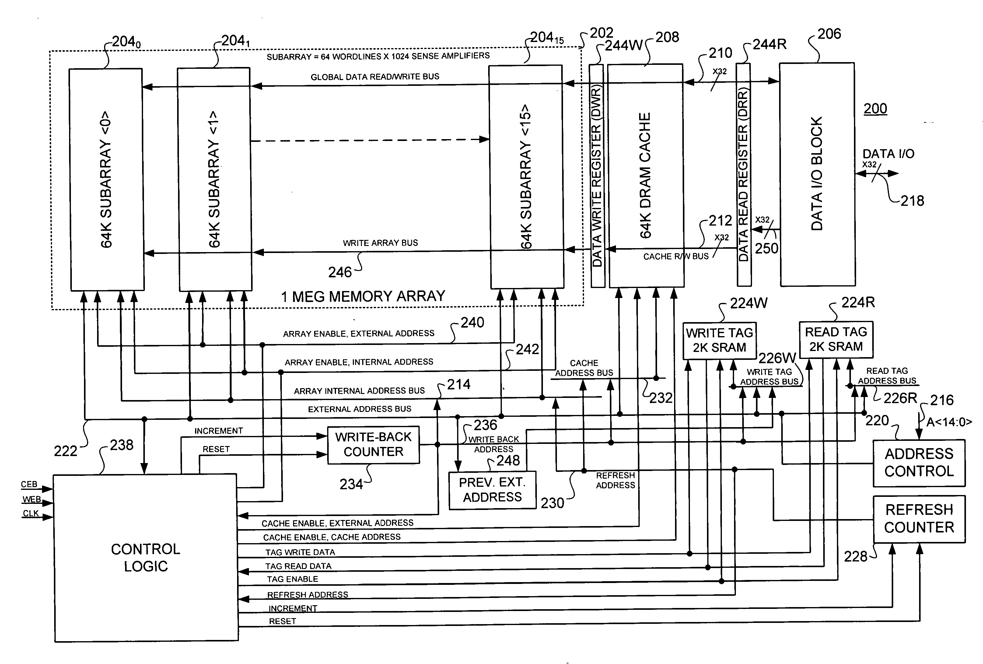
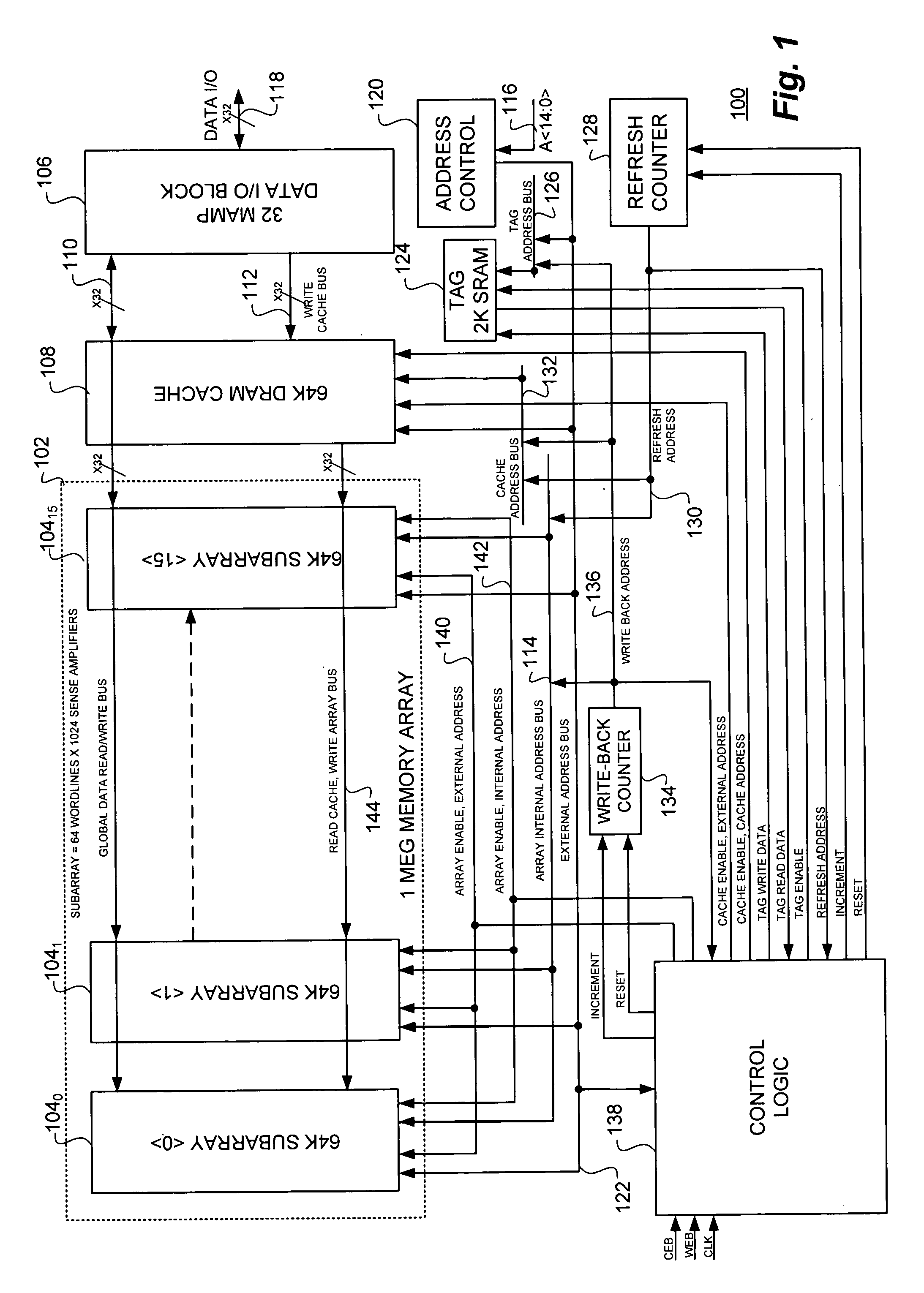
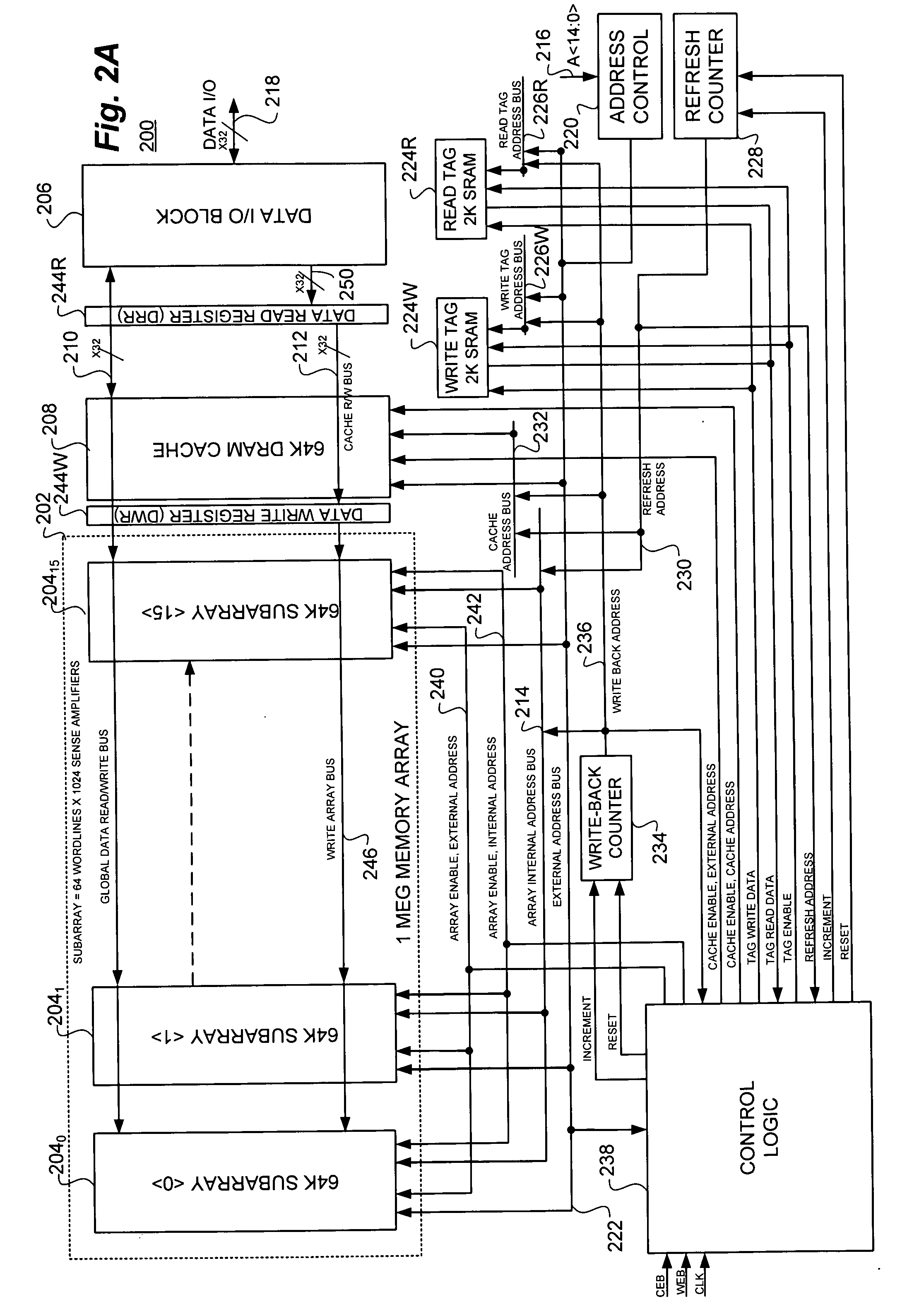
[0054] With reference now to FIG. 1, a functional block diagram of a memory 100 as disclosed in the aforementioned United States Patent is shown wherein refresh of the subarrays and cache may be effectuated in parallel with any combination of external accesses and control logic and control signals may be thereby used to hide refresh operations in the memory array.

[0055] The memory 100 comprises, in the representative implementation illustrated, a 1 Meg memory array 102 comprising sixteen 64 K subarrays 1040 through 10415 (subarray 0> through subarray 15>). A data I / O block 106 is coupled to a 64 K DRAM cache 108 as well as the subarrays 1040 through 10415 by a global data read / write bus 110. A read cache, write array bus 144 couples the DRAM cache 108 to the subarrays 1040 through 10415. Write cache bus 112 couples the data I / O block 106 and the DRAM cache 108. The DRAM cache 108 may be the same size as each of the subarrays 1040 through 10415.

[0056] An array internal address bus ...


PUM


Abstract

A high-speed, static random access memory (SRAM) compatible, high availability memory array and method employing synchronous dynamic random access memory (DRAM) in conjunction with a data cache and separate data read and write registers and tag blocks. The inclusion of separate data read and write registers allows the device to effectively operate at a cycle time limited only by the DRAM subarray cycle time. Further, the inclusion of two tag blocks allows one to be accessed with an externally supplied address and the other to be accessed with a write-back address, thus eliminating the requirement for a single tag to execute two read-modify write cycles in one DRAM cycle time.

Description

CROSS REFERENCE TO RELATED PATENT APPLICATIONS [0001] The present invention is related to the subject matter disclosed in U.S. patent application Ser. No. [UMI-361] filed on DDMMYY for: “Static Random Access Memory (SRAM) Compatible, High Availability Memory Array and Method Employing Synchronous Dynamic Random Access Memory (DRAM) in Conjunction with a Single DRAM Cache and Tag”, assigned to the assignee of the present invention, the disclosure of which is herein specifically incorporated by this reference in its entirety.COPYRIGHT NOTICE / PERMISSION [0002] A portion of the disclosure of this patent document contains material which is subject to copyright protection. The copyright owner has no objection to the facsimile reproduction by anyone of the patent document of the patent disclosure as it appears in the United States Patent and Trademark Office patent file or records, but otherwise, reserves all copyright rights whatsoever. The following notice applies to the software and dat...

Claims


Application Information

Patent Timeline
Patent Type & Authority Applications(United States)
IPC IPC(8): G06F13/28
CPCG06F12/0804G11C11/406G11C11/40607G11C11/4076
Inventor BUTLER, DOUGLAS BLAINEJONES, OSCAR FREDERICK JR.PARRIS, MICHAEL C.HARDEE, KIM C.
Owner INVENSAS CORP
Why Eureka
Try Eureka