Light emitting diode package including monitoring photodiode

a technology of light-emitting diodes and photodiodes, applied in the direction of instruments, material analysis through optical means, milking devices, etc., can solve the problems of heightened optical connection efficiency, physical separation, and alteration of light output and peak wavelength by own heat generation, and achieve the effect of enhancing reliability

Active Publication Date: 2006-08-31
SAMSUNG ELECTRONICS CO LTD
View PDF2 Cites 31 Cited by
  • Summary
  • Abstract
  • Description
  • Claims
  • Application Information

AI Technical Summary

Benefits of technology

[0010] The present invention has been made to solve the foregoing problems of the prior art and it is therefore an object of the present invention to provide a Light Emitting Diode (LED) package including photo diode by replacing a submount substrate with a silicon substrate for LED packaging and forming a photo diode in the silicon substrate to enhance reliability with respect to optical connection efficiency and optical output detection.
[0018] Preferably, to improve optical connection efficiency for photo diode, the LED chip has a light-emitting area placed corresponding to the light-receiving area of the photo diode. The photo diode can be formed via an impurity diffusion process or an epitaxial layer growth process.
[0023] Also, the light-receiving area of the photo diode may comprise a partially reflective film having a low light transmittance in accordance with desired light quantity. According to the invention, the photo diode is configured as a single package in the LED, and thus by receiving light partially through the partially reflective film, better optical connection efficiency is attainable compared with a conventional method.
[0024] The partially reflective film may have a reflectivity of 70% to 90% to prevent decrease in light extraction efficiency of the LED. The partially reflective film may be made of a material selected from a group consisting of SiO2, TiO2, Si3N4, ZrO2 and HfO2, and a proper thickness of the film ensures desired optical properties. The partially reflective film may be made of an insulating material. If the film is made of the insulating material, the partially reflective film may be integrally formed with the insulation layer to serve as an insulation layer portion having a partially reflective function.
[0025] The photo diode employed in this invention is configurable as various structures that can be formed in the silicon substrate, and the connecting terminal of the photo diode can be varied adequately according to each structure.

Problems solved by technology

However, the LED has disadvantages in that temperature change resulting from its own heat generation alters light output and peak wavelength.
But such an arrangement according to the reference cited inevitably causes physical separation since an LED package and a photo diode package are arranged separately on the lead frame.
This renders it unlikely that optical connection efficiency is heightened.
In addition, since a great deal of noise may interfere with the detected light due to change in other external environments, it is hard to expect high reliability.

Method used


Image

  • Light emitting diode package including monitoring photodiode
  • Light emitting diode package including monitoring photodiode
  • Light emitting diode package including monitoring photodiode

Examples


first embodiment

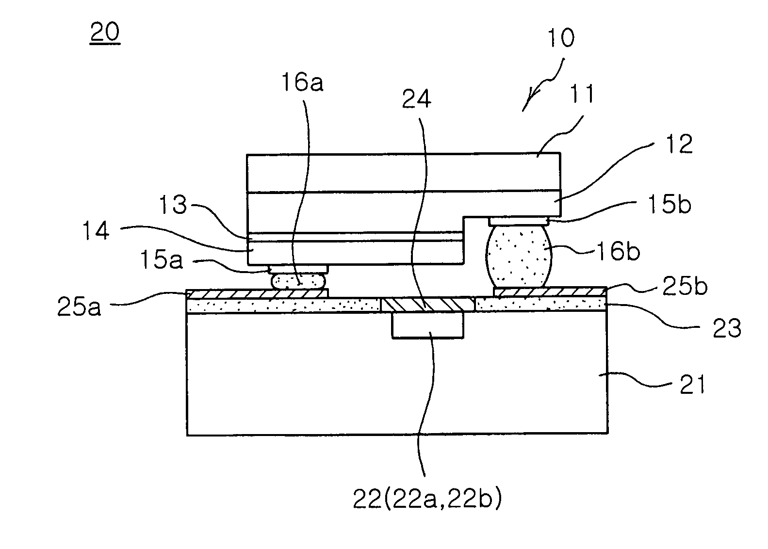
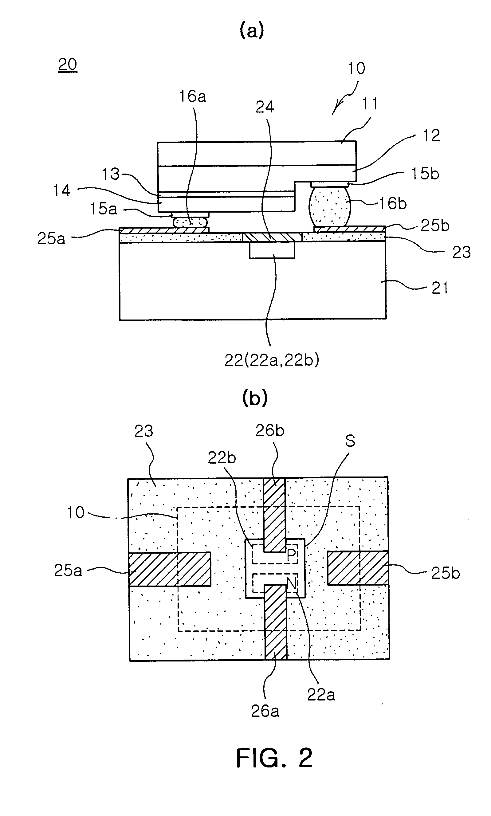
[0037]FIG. 2a is a sectional view of a Light Emitting Diode (LED) package according to the invention.

[0038] The LED package 20 shown in FIG. 2a includes a silicon substrate 21 having a photo diode 22 provided in an upper part, and an LED chip 10 mounted on the silicon substrate 21. The photo diode 22 may be a PIN structure including p- and n-type impurity areas 22a, 22b formed via a diffusion process in an area of the upper part of the silicon substrate 21. The embodiment of the invention depicts forming the photo diode via a diffusion process, which however can be formed via a typical epitaxial layer growth process, as is easily understood by those skilled in the art.

[0039] The LED chip 10 includes a first conductivity-type semiconductor layer 12, an active layer 13 and a second conductivity-type semiconductor layer 14, which are sequentially formed on a substrate 11. According to the embodiment of the invention, the LED chip 10 has a planar structure in which first and second ele...

second embodiment

[0046]FIG. 3a is a sectional view of the LED package according to the invention.

[0047] The LED package 40 shown in FIG. 3a includes a silicon substrate configured as a photo diode and an LED chip 30 mounted on the silicon substrate 41. The silicon substrate 41 can be provided as the photo diode 42 by forming an intrinsic area and an n-type impurity area in an area of the upper part of the first conductivity-type silicon substrate 41 via a diffusion process.

[0048] An LED chip 30 includes a first conductivity-type semiconductor layer 34, an active layer 33 and a second conductivity-type semiconductor layer 34 sequentially formed on a substrate 31. First and second electrodes 35a,35b have a planar structure facing one direction. Further, an insulation layer 43 is formed on the silicon substrate 41 excluding at least a light-receiving area of the photo diode 42. A partially reflection film 44 may be formed on the light-receiving area of the photo diode 42.

[0049] As shown in FIG. 3b, t...

third embodiment

[0052]FIG. 4a is a sectional view of the LED package according to the invention.

[0053] An LED package 60 shown in FIG. 4a includes a silicon substrate 61 having a photo diode 62 in an upper part thereof, and an LED chip 50 mounted on the silicon substrate 61. The photo diode 62 may be a PIN structure having p-and n-type impurity areas 62a,62b formed on an area of an upper part of the silicon substrate 61 via a diffusion process.

[0054] An LED chip 50 includes a first conductivity-type semiconductor layer 52, an active layer 53 and a second conductivity-type semiconductor layer 54 sequentially formed on the substrate 51 in a manner similar to the embodiment described above. However, the LED chip 50 employed in the embodiment has a vertical structure in which first and second electrodes 55a,55b are arranged on opposed faces.

[0055] An insulation layer 63 is formed on the silicon substrate 61 excluding at least a light-receiving area S1 of the photo diode 62. A partially reflective fil...


PUM


Abstract

The present invention relates to an LED package including photo diode. The LED package includes a silicon substrate, and a photo diode is formed in an upper part thereof. Also, an insulation layer is formed on the silicon substrate excluding at least a light-receiving area of the photodiode. In the LED package, an LED terminal is formed on the insulation layer to be connected to the photo diode. First and second LED connecting pads are formed on the insulation layer, and arranged on both sides of the photo diode. In addition, an LED chip is mounted on the silicon substrate, and connected to the first and second LED connecting pads.

Description

CLAIM OF PRIORITY [0001] This application claims the benefit of Korean Patent Application No. 2005-16151 filed on Feb. 25, 2005, in the Korean Intellectual Property Office, the disclosure of which is incorporated herein by reference. BACKGROUND OF THE INVENTION [0002] 1. Field of the Invention [0003] The present invention relates to a Light Emitting Diode (LED) package. More particularly, the present invention relates to the LED package including photo diode which detects actual quantity of output light to stabilize light output. [0004] 2. Description of the Related Art [0005] Recently a Light Emitting Diode (LED) has been used as a next-generation lighting source due to its higher-power and higher efficiency compared with other light sources. In general, unlike light source for a simple indicator, lighting source is required to maintain stability of light output. However, the LED has disadvantages in that temperature change resulting from its own heat generation alters light output...

Claims


Application Information

Patent Timeline
Patent Type & Authority Applications(United States)
IPC IPC(8): H01L31/00H01L27/15H01L33/62
CPCH01L25/167H01L31/147H01L2224/48091H01L2224/48137H01L2924/00014H01L2224/48139A01J5/16
Inventor LEE, SUNG JUNHWANG, WOONG LINCHOI, SEOG MOONPARK, HO JOONCHOI, SANG HYUNLIM, CHANG HYUN
Owner SAMSUNG ELECTRONICS CO LTD
Why Eureka
Try Eureka