Integrated circuit, and method for the production of an integrated circuit

a technology of integrated circuits and integrated circuits, applied in thermoelectric devices, plastic/resin/waxes insulators, coatings, etc., can solve the problems of high process cost, low throughput, and high temperature of inorganic nitrides, and achieve high process cost or high temperatur

Inactive Publication Date: 2006-09-14
INFINEON TECH AG
View PDF21 Cites 7 Cited by
  • Summary
  • Abstract
  • Description
  • Claims
  • Application Information

AI Technical Summary

Benefits of technology

[0022] It is advantageous if at least one base polymer is a phenol-containing polymer or copolymer, in particular poly-4-vinylphenol, poly-4-vinylphenol-co-2-hydroxyethyl methacrylate or poly-4-vinylphenol-co-methyl methacrylate.

Problems solved by technology

However, the high process costs and the low throughput are disadvantageous for mass-produced products.
Similarly to the preparation of inorganic oxides, the deposits of inorganic nitrides require high temperatures or high process costs.
However, this crosslinking is effected at temperatures of 200° C, which is problematic for the production of flexible substrates having a large area.

Method used


Image

  • Integrated circuit, and method for the production of an integrated circuit
  • Integrated circuit, and method for the production of an integrated circuit
  • Integrated circuit, and method for the production of an integrated circuit

Examples


Embodiment Construction

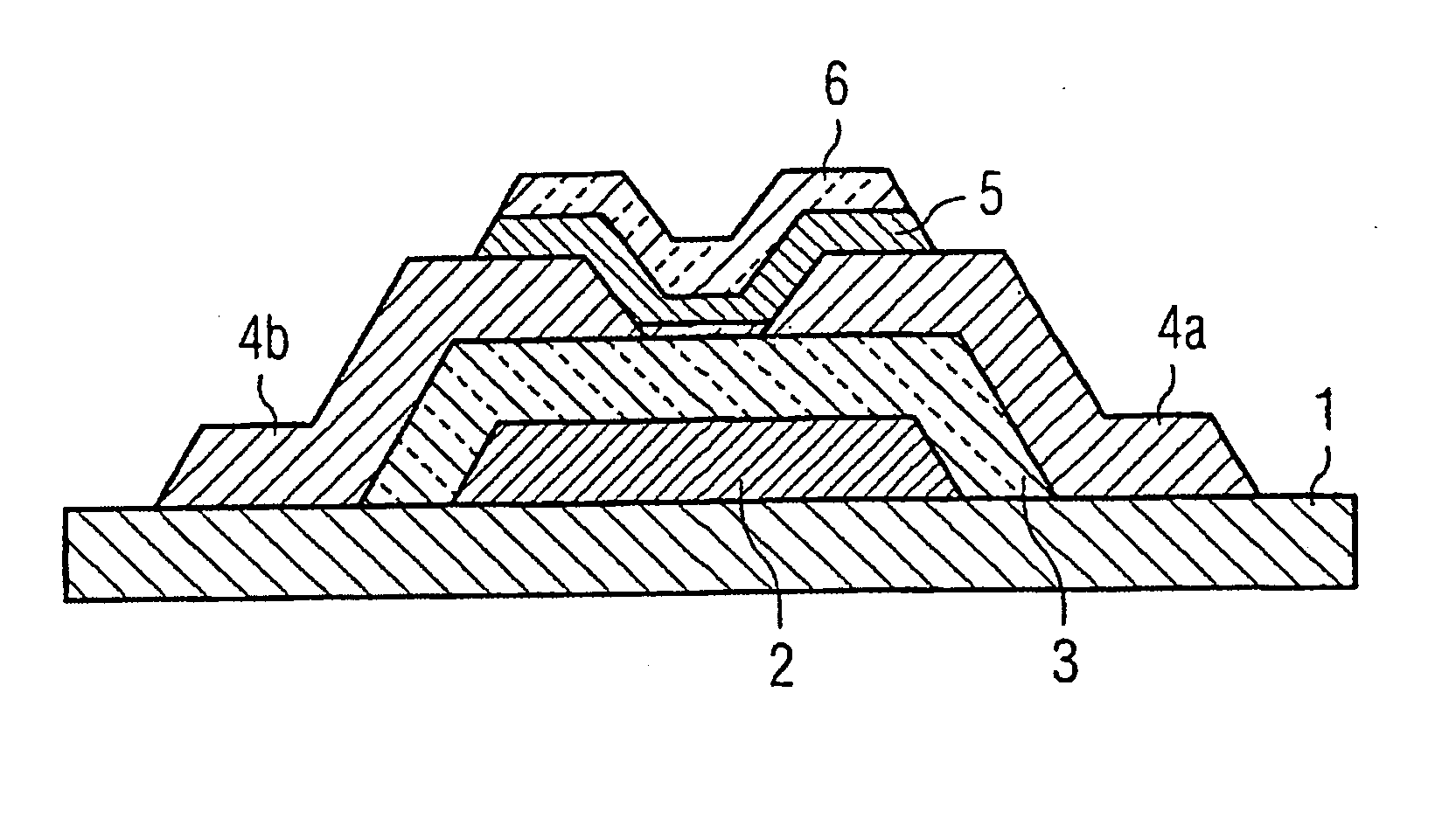
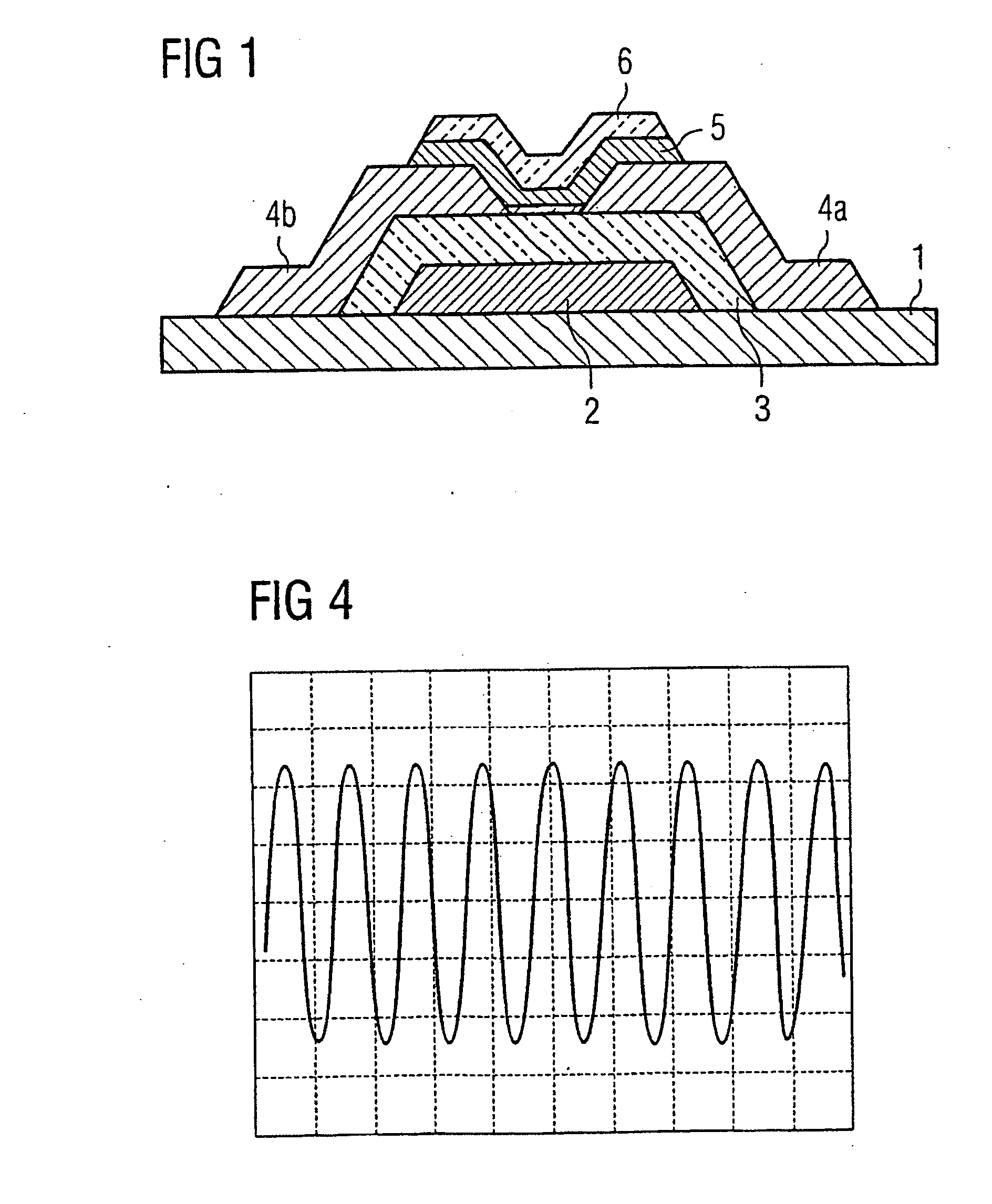
[0050] OFETs are electronic components that consist of a plurality of layers, all of which have been structured in order to generate integrated circuits by connections of individual layers. FIG. 1 shows the fundamental structure of an OFET transistor in a bottom contact architecture.

[0051] A gate electrode 2, which is covered by a gate dielectric layer 3, is arranged on a substrate 1. As will be explained later, in an embodiment of the process according to the invention the substrate 1 with the gate electrode 2 already arranged thereon constitutes the starting material on which the gate dielectric layer 3 is applied. A drain layer 4a and a source layer 4b, both of which are connected to the active semiconducting layer 5, are arranged on the gate dielectric layer 3. A passivating layer 6 is arranged above the active-layer 5.

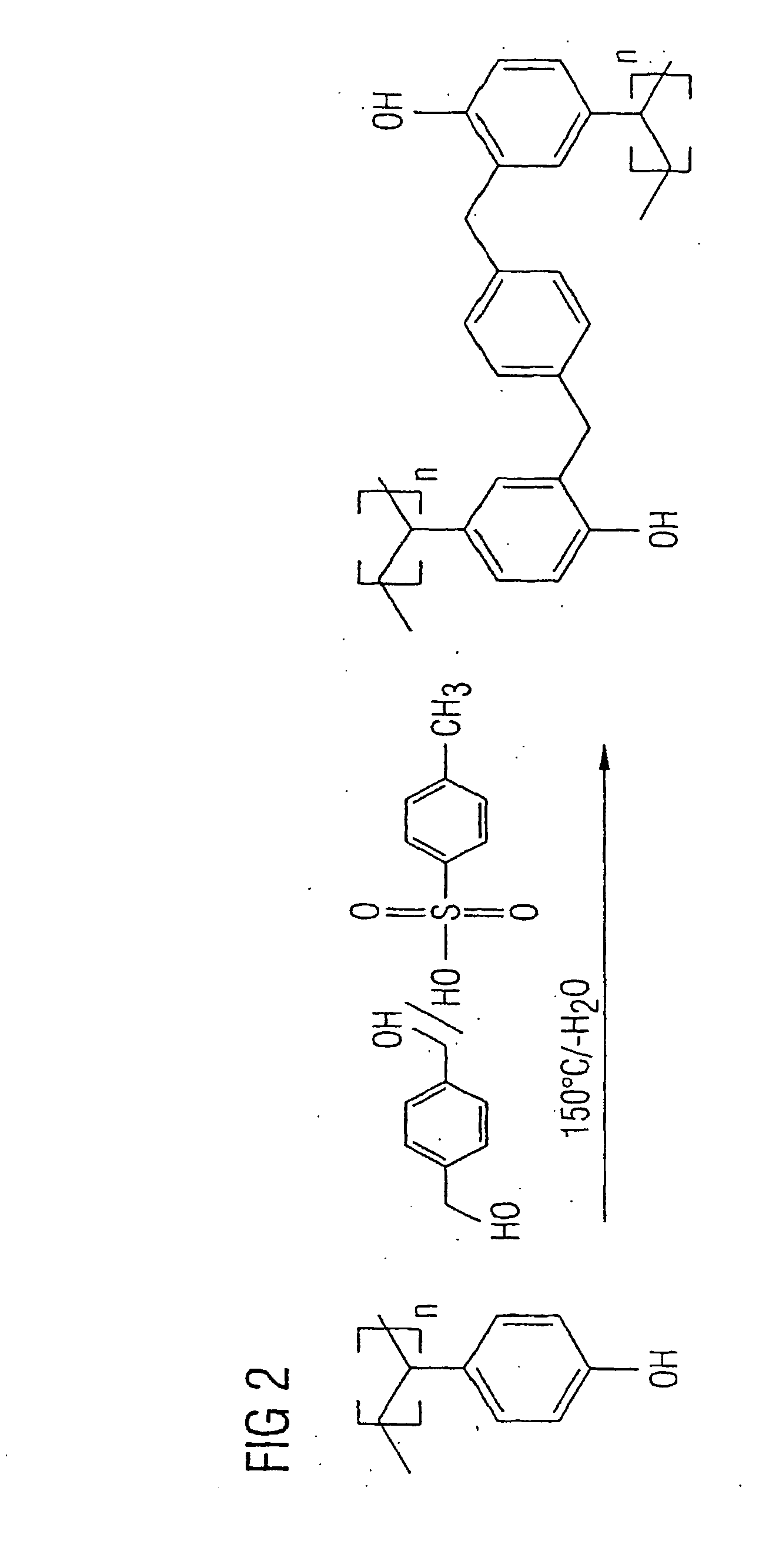
[0052] The deposition and processing of the gate dielectric layer 3 are described herein below.

[0053] The circuits according to embodiments of the invention an...


PUM

PropertyMeasurementUnit
temperaturesaaaaaaaaaa
temperatureaaaaaaaaaa

Abstract

Embodiments of the invention relate to an integrated circuit comprising an organic semiconductor, particularly an organic field effect transistor (OFET) that is provided with a dielectric layer. The integrated circuit is produced by means of a polymer formulation consisting of a) 100 parts of at least one crosslinkable basic polymer, b) 10 to 20 parts of at least one electrophilic crosslinking component, c) 1 to 10 parts of at least one thermal acid catalyst that generates an activating proton at temperatures ranging from 100 to 150° C., dissolved in d) at least one solvent. Other embodiments of the invention further relate to a method for producing an integrated circuit, which makes it possible to produce integrated circuits comprising dielectric layers, especially for OFET's at low temperatures.

Description

[0001] This application is a continuation of co-pending International Application No. PCT / DE2004 / 001904, filed Aug. 24, 2004, which designated the United States and was not published in English, and which is based on German Application No. 103 40 609.3, filed Aug. 29, 2003, both of which applications are incorporated herein by reference.TECHNICAL FIELD [0002] The invention relates to an integrated circuit and a method for producing an integrated circuit comprising an organic semiconductor. BACKGROUND [0003] Systems comprising integrated circuits based on organic field effect transistors (OFET) constitute a promising technology in the mass application sector of economical electronics. A field effect transistor is considered to be organic particularly if the semiconducting layer is produced from an organic material. [0004] Since it is possible to build up complex circuits using OFETs, there are numerous potential applications. Thus, for example, the introduction of RF-ID (radio freque...

Claims


Application Information

Patent Timeline
Patent Type & Authority Applications(United States)
IPC IPC(8): H01L29/08C08K5/053C08K5/42C08L61/14H01B3/44H01L51/30
CPCH10K10/471C08G61/02C08G2261/42C08G2261/1422C08G2261/334C08F8/00C08F2810/20C09D129/04C08F216/06C08K5/053C08K5/42C08L61/14
Inventor HALIK, MARCUSKLAUK, HAGENSCHMID, GUENTERWALTER, ANDREASZSCHIESCHANG, UTE
Owner INFINEON TECH AG
Why Eureka
Try Eureka