Method for manufacturing an electrolyte material layer in semiconductor memory devices

Inactive Publication Date: 2006-09-14
ADESTO TECH
View PDF6 Cites 10 Cited by
  • Summary
  • Abstract
  • Description
  • Claims
  • Application Information

AI Technical Summary

Benefits of technology

[0022] Therefore, the present invention provides a non-volatile memory cell on the basis of CMOS technology with a fast, scalable, low-voltage switching mechanism and a high switching

Problems solved by technology

However, these memory concepts based on charge storage have some general drawbacks like high voltage operation (10-20V), slow programming speed (between μs and ms) and a limited programming endurance (typically 105-106 write/erase cycles).
Due to the required high voltages, high power consumption is needed for programming and erasing FLASH memories.
The existence of such an energy barrier thus severely limits the performance and the scalability of these devices.
These facts imply several severe restrictions regarding the system design.
Since charge storage memories (e.g., DRAM and floating gate memories like FLASH) are reaching their scaling limits due to data retention problems caused by inevitable charge leakage from the cells, and moreover, poor data sensing capability of the ever-decreasing amounts of stored charge, alternative electronic switchin

Method used


Image

  • Method for manufacturing an electrolyte material layer in semiconductor memory devices
  • Method for manufacturing an electrolyte material layer in semiconductor memory devices
  • Method for manufacturing an electrolyte material layer in semiconductor memory devices

Examples


Embodiment Construction

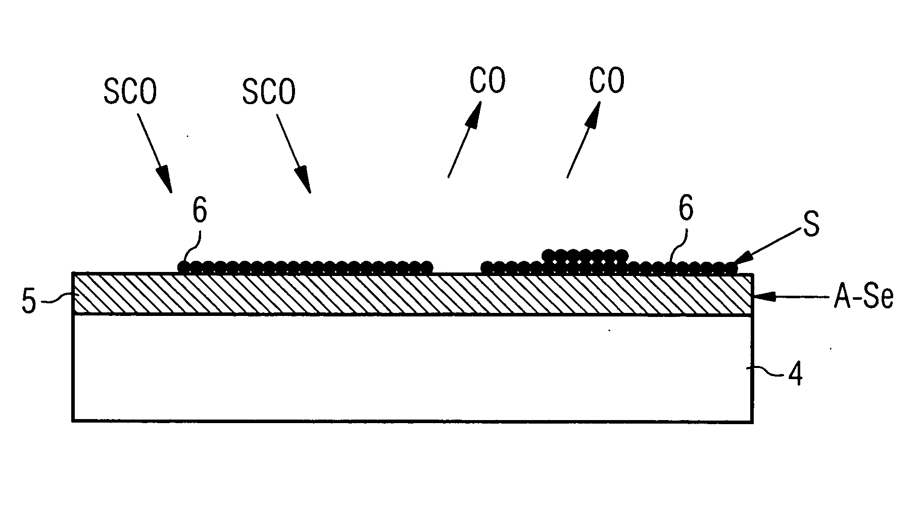
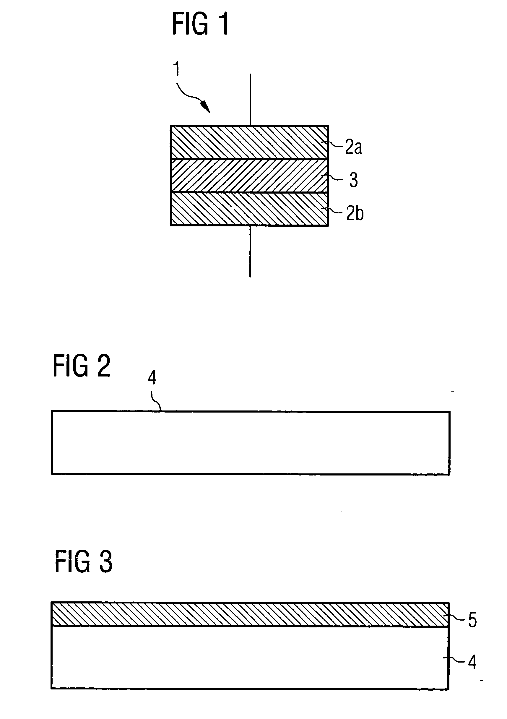
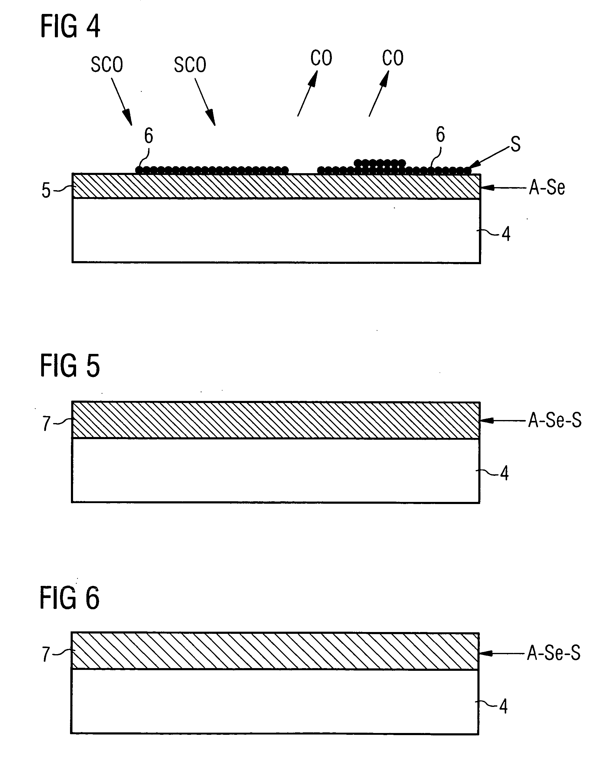
[0053]FIG. 1 is a schematic representation of a section through a resistively switching memory cell according to prior art. It comprises two corresponding metal electrodes 2a, 2b (i.e., one anode and one cathode), between which a corresponding, electrochemical “electrolyte” material layer 3 comprising a chalcogenide compound is positioned which is adapted to be set, by appropriate switching processes, in a more or less conductive state.

[0054] For programming the resistively switching memory cell 1 (depending on whether a logic “One” or a logic “Zero” is to be written into the memory cell 1), appropriate current pulses are applied to the electrodes 2a, 2b and electrochemical reactions in the electrolyte chalcogenide material layer 3 are caused by the pulses, which result in a conductive state or a non-conductive state of the cell 1. Due to the resistive switching mechanism, a metallic connection / clusters between electrodes 2a, 2b is either built up, or dissolved depending on whether...


PUM


Abstract

A method for manufacturing an electrolyte material layer with a chalcogenide material incorporated or deposited therein for use in semiconductor memory devices, in particular resistively-switching memory devices or components. The method comprises the steps of producing a semiconductor substrate, depositing a binary chalcogenide layer onto the semiconductor substrate, depositing a sulphur-containing layer onto the binary chalcogenide layer, and creating a ternary chalcogenide layer comprising at least two different chalcogenide compounds ASexSy. One component A of the chalcogenide compounds ASexSy comprises materials of the IV elements main group, e.g., Ge, Si, or of a transition metal, preferably of the group consisting of Zn, Cd, Hg, or a combination thereof.

Description

FIELD OF THE INVENTION [0001] The invention refers to a method for manufacturing an electrolyte material layer comprising chalcogenide compound in semiconductor memory devices. In more detail, the invention refers to a method for manufacturing a chalcogenide compound for using as an electrolyte material layer in semiconductor memory devices or components, in particular resistively switching memories, and to memory devices manufactured by that method. BACKGROUND OF THE INVENTION [0002] In memory components, in particular semiconductor memory components, a distinction is made between so-called functional memory components, e.g., PLAs, PALs etc. and so-called tab memory components, e.g., ROM components (ROM=Read Only Memory), for example PROMs, EPROMs, EEPROMs, and Flash-memories, and RAM components (RAM=Random Access Memory), e.g., DRAMs or SRAMs (D=dynamic, S=static). [0003] A RAM component is a memory device in which data is stored under a specific address, from which the data can b...

Claims


Application Information

Patent Timeline
IPC IPC(8): H01L21/06H01L21/20H01L21/8238H01L21/00
CPCH01L45/085H01L45/141H01L45/142H01L45/143H01L45/146H01L45/1616H01L45/1625H01L45/1641H10N70/245H10N70/8822H10N70/882H10N70/8825H10N70/023H10N70/8833H10N70/041H10N70/026G11C13/0004
Inventor PINNOW, CAY-UWEUFERT, KLAUS-DIETER
Owner ADESTO TECH
Why Eureka
Try Eureka