Method of fabricating a non-volatile memory element

Inactive Publication Date: 2006-09-14
RENESAS ELECTRONICS CORP
View PDF11 Cites 6 Cited by
  • Summary
  • Abstract
  • Description
  • Claims
  • Application Information

AI Technical Summary

Benefits of technology

[0022] According to the present invention, it is made possible to prevent the trap sites from generating in the insulating film and to improve the film quality, by forming the insulating film in contact with

Problems solved by technology

It was finally found that the technique described in the above patent document was insufficient in terms of effect of modifying the film quality.
More specifically, the method described in the above patent publication allowed only nitriding reaction to proceed in modification of the film qua

Method used


Image

  • Method of fabricating a non-volatile memory element
  • Method of fabricating a non-volatile memory element
  • Method of fabricating a non-volatile memory element

Examples


first embodiment

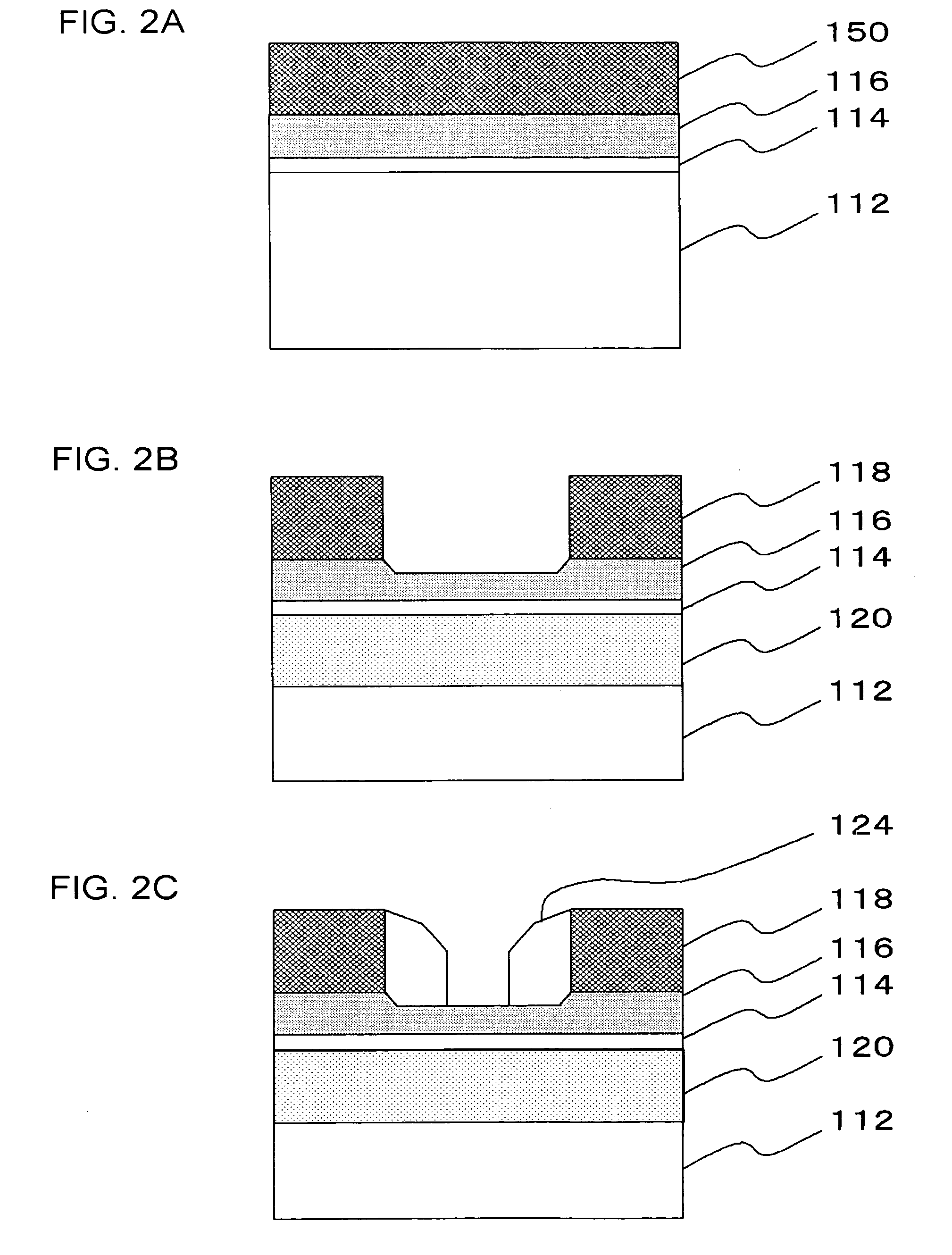
[0068] As has been described in the above, the interpoly insulating film 134 is formed after the floating gate 101 is processed. In this embodiment, the interpoly insulating film 134 is formed by exposing, after formation of the HTO film (Step 201), the HTO film simultaneously to a nitrogen-containing gas and oxygen, to thereby introduce nitrogen into the HTO film and thicken it (Step 202).

[0069] The interpoly insulating film 134 is formed by the CVD process. More specifically, a Si-containing gas and an oxygen-containing gas are used as film-forming gases in an LP furnace (reduced-pressure CVD furnace), and the HTO (high temperature oxide) film is grown under a reduced pressure of 150 Pa or lower, and at a temperature of 750° C. or above, and more preferably approximately 800° C. to 850° C. The thickness of the HTO film may be of any desired value, typically in the range from 8 nm to 20 nm, both ends inclusive. SiH4 or SiHCl2 is typically used as the Si-containing gas. N2O is typi...

second embodiment

[0088] Of the process steps of fabricating the non-volatile memory element 110 shown in FIG. 1, the annealing for modifying the HTO film which serves as the interpoly insulating film 134 may be carried out in an atmosphere further containing N2 gas, in addition to NO or N2O gas in combination with O2 gas.

[0089] In this embodiment, N2 is added for dilution in order to adjust the rate of oxidation. This makes it possible to suppress the amount of increase in the thickness of the HTO film, while keeping the modification effect by the annealing. This is because the N2 dilution does not largely alter the amount of introduction of nitrogen ascribable to NO gas, but the oxidation is suppressed by the dilution. According to the method of modification in this embodiment, it is therefore made possible to independently and arbitrarily control the amount of thickening of the HTO film due to oxidation. The roughness of the interface of the interpoly insulating film 134 can therefore be decrease...

third embodiment

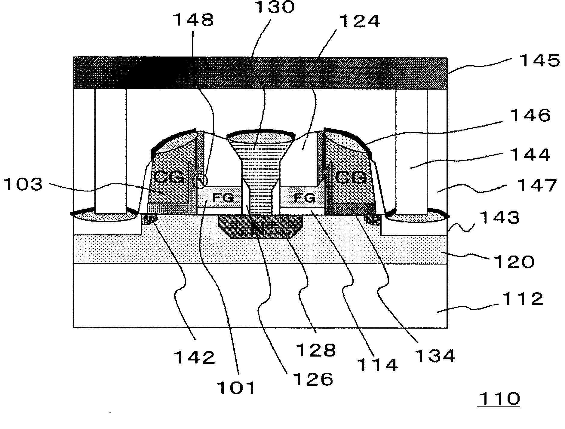
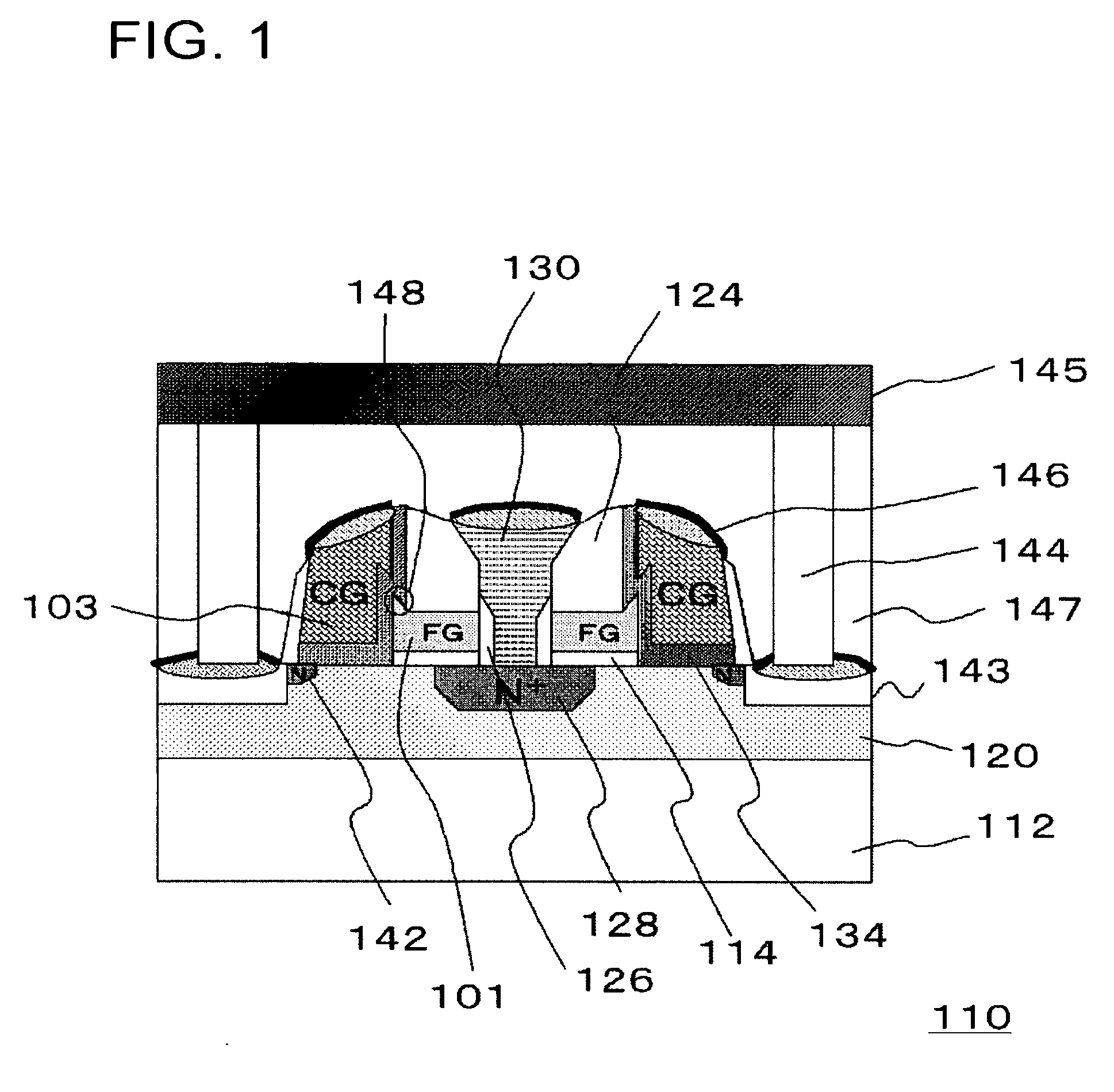
[0090]FIG. 6 is a drawing showing another embodiment of the non-volatile memory element 110. In FIG. 6, the floating gate FG 101 is provided on the silicon substrate 112 while placing the silicon oxide film 114 in between, and a source / drain region 160 is provided adjacent to the floating gate FG 101. On the floating gate FG 101, the control gate CG 103 is provided while placing the interpoly insulating film 134 in between.

[0091] The methods of growing the interpoly insulating film 134 explained in the first embodiment and the second embodiment are adoptable also to formation of the interpoly insulating film 134 in the non-volatile memory element 110 having the control gate CG 103 formed on the floating gate FG 101 as shown in FIG. 6.

[0092] The present invention has been described in the above referring to the embodiments, wherein the embodiments are merely of exemplary purposes, so that it will be readily understood by those skilled in the art that various modifications are allow...


PUM


Abstract

An interpoly insulating film is modified in the film quality, while preventing generation of trap sites. A floating gate 101 is provided on a channel-forming region in the vicinity of the surface of a silicon substrate 112, an interpoly insulating film 134 is provided so as to contact with the floating gate 101, and a control gate 103 is provided so as to contact with the interpoly insulating film 134 and so as to be opposed to at least a part of the floating gate 101. A process step of providing the interpoly insulating film 134 further includes a step of forming on the floating gate 101, the interpoly insulating film 134 so as to contact with the floating gate 101, and a step of exposing, subsequently to the formation of the interpoly insulating film 134, the interpoly insulating film 134 to an atmosphere containing a nitrogen-containing gas and oxygen, to thereby simultaneously proceed nitriding and oxidation of the interpoly insulating film 134.

Description

[0001] This application is based on Japanese patent application No. 2005-064628 the content of which is incorporated hereinto by reference. BACKGROUND [0002] 1. Technical Field [0003] The present invention relates to a technique of modifying quality of an insulating film in a non-volatile memory element. [0004] 2. Related Art [0005] In a non-volatile memory element configured as having a floating gate and a control gate disposed while placing an interpoly insulating film in between, data writing is accomplished when hot electrons generated in a channel region on a substrate are incorporated into the floating gate. Data is erased when the electrons are drawn out from the floating gate into the control gate based on the F-N (Fowler-Nordheim) tunneling phenomenon. [0006] The non-volatile memory element having the interpoly insulating film between the floating gate and the control gate as described in the above has been known to suffer from a problem in that repetitive writing and erasu...

Claims


Application Information

Patent Timeline
IPC IPC(8): H01L21/336
CPCH01L21/28273H01L21/3145H01L27/115H01L27/11521H01L29/7885H01L29/40114H01L21/02249H10B69/00H10B41/30
Inventor MAKABE, MARIKOHASEGAWA, EIJI
Owner RENESAS ELECTRONICS CORP
Why Eureka
Try Eureka