Fusing nanowires using in situ crystal growth

a nanowire and crystal growth technology, applied in the field of nanotechnology, can solve the problems of unplanned high aggregate resistance, poor electrical, and relative high aggregate resistivity, and achieve the effect of facilitating interconnection between nanostructures

Inactive Publication Date: 2006-09-14
HEWLETT PACKARD DEV CO LP
View PDF3 Cites 27 Cited by
  • Summary
  • Abstract
  • Description
  • Claims
  • Application Information

AI Technical Summary

Benefits of technology

[0008] In some embodiments of the present invention, a method of interconnecting nano-structures is provided. The method of interconnecting comprises performing crystal growth in situ on prefabricated nano-structures immersed in a growth solution having a controllable saturation condition, such that interconnection between the nano-structures is facilitated.
[0012] In other embodiments of the present invention, an ink formulation for an inkjet printer is provided. The ink formulation comprises a plurality of nano-structures and a growth solution. The growth solution comprises a crystal material dissolved in a solvent. The crystal material has a characteristic in common with a material of the nano-structures. The plurality of nano-structures is suspended in the growth solution. The growth solution is manipulatable to facilitate fusing of the plurality of nano-structures on a substrate that uses the crystal material of the solution.

Problems solved by technology

Unfortunately, individual nanowires and nanoparticles deposited on a substrate as either a linear, wire-like form or a planar film often exhibit a relatively high aggregate resistivity as a deposited structure.
Such point contacts make for poor electrical as well as mechanical interfaces between deposited nanowires leading to an unexpectedly high aggregate resistance.

Method used


Image

  • Fusing nanowires using in situ crystal growth
  • Fusing nanowires using in situ crystal growth
  • Fusing nanowires using in situ crystal growth

Examples


Embodiment Construction

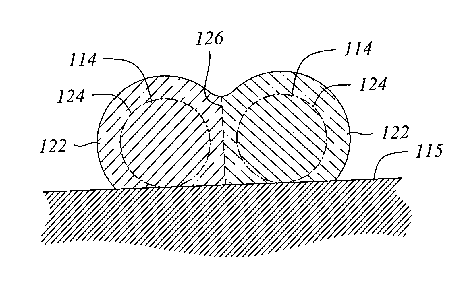
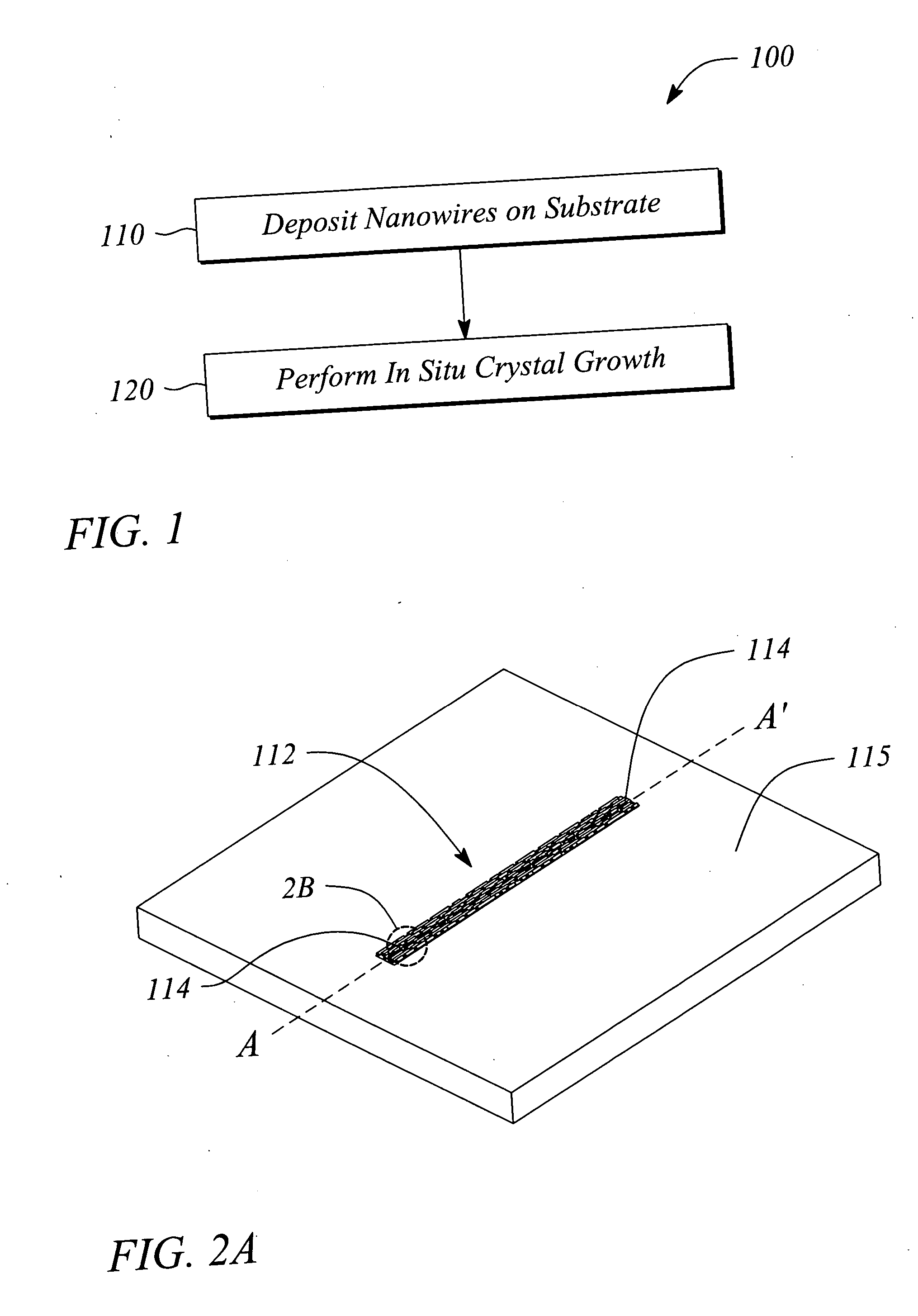
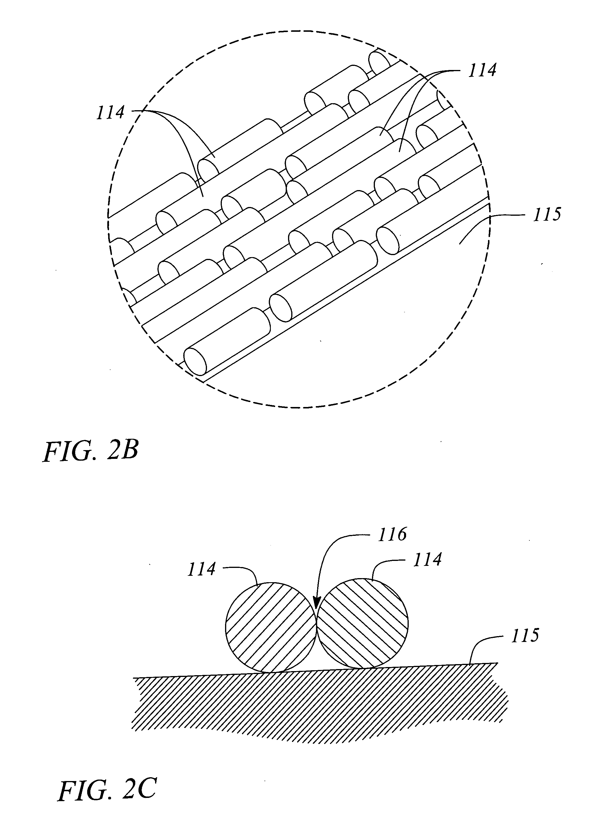
[0030] The embodiments of the present invention facilitate interconnecting nano-structures including, but not limited to, nanowires, nanoparticles and combinations thereof. Hereinafter, the term ‘nanowires’ or ‘nano-structures’ will be used to generally refer to one or both of nanowires and nanoparticles, without limitation. Moreover, examples and embodiments described herein may refer to ‘nanowires’ and are intended to apply equally to nano-structures including, but not limited to, nanoparticles and combinations of nanowires and nanoparticles. In some embodiments, interconnections between nanowires deposited on a substrate as a cluster or aggregated structure are formed where an interconnection was not previously present. In some embodiments, interconnections between nanowires deposited on a substrate as a cluster or aggregated structure are strengthened and / or improved when pre-existing interconnections are present. By ‘strengthened’ and / or ‘improved’, it is meant that at least on...


PUM


Abstract

Crystal growth performed in situ facilitates interconnection of prefabricated nano-structures. The nano-structures are immersed in a growth solution having a controllable saturation condition. Changing the saturation condition of the solution modifies a size of the immersed nanowires. The solution includes a solute of a nano-structure precursor material. The saturation condition is changed to one or both etch material from a surface of the nano-structures and initiate crystal growth on the nano-structure surface. A nano-structure interconnection system includes the growth solution and equipment to deposit the prefabricated nano-structures on a substrate. An interconnected structure includes a plurality of nano-structures disposed on a substrate in a cluster and a liquid phase-grown crystal lattice on surfaces of the nano-structures to form physical interconnections between the plurality. An ink formulation includes the plurality of nano-structures suspended in the growth solution.

Description

BACKGROUND [0001] 1. Technical Field [0002] The invention relates to nanotechnology. In particular, the invention relates to structures having nano-scale feature sizes fabricated using nano-structures. [0003] 2. Description of Related Art [0004] Nanotechnology is concerned with the fabrication and application of so-called nano-scale, crystalline structures, structures having at least one linear dimension between 1 nm and 200 nm. These nano-scale crystalline structures are often 50 to 100 times smaller than conventional semiconductor structures. Hereinafter, a nano-scale, crystalline structure may be referred to as a ‘nano-structure’ that includes, but is not limited to, a nanoparticle and a nanowire. Nanoparticles and nanowires are individual, low dimensional, nano-scale, crystalline structures. Specifically, nanoparticles are generally characterized as having three quantum confined dimensions or directions (i.e., width, height, and length) while nanowires typically are characterize...

Claims


Application Information

Patent Timeline
Patent Type & Authority Applications(United States)
IPC IPC(8): H01L21/00
CPCB82Y10/00B82Y30/00H01L29/0665H01L27/1292H01L29/0673H01L29/78696H01L29/0669
Inventor PAN, ALFREDJEON, YOOCHARNNG, HOU T.HAUBRICH, SCOTT
Owner HEWLETT PACKARD DEV CO LP
Why Eureka
Try Eureka