Semiconductor device and manufacturing method for semiconductor device

a semiconductor device and semiconductor technology, applied in the field of semiconductor devices, can solve the problems of gate oxide film easily breaking, conventional semiconductor devices cannot solve, and great obstacles to the application of high-speed switching elements, so as to prevent the breakdown of gate oxide film and reduce the gate capacitance

Active Publication Date: 2006-09-21
RENESAS ELECTRONICS CORP
View PDF4 Cites 13 Cited by
  • Summary
  • Abstract
  • Description
  • Claims
  • Application Information

AI Technical Summary

Benefits of technology

[0021] According to the present invention, it is possible to provide semiconductor device capable of reducing a gate capacitance, and preventing breakdown of a gate oxide film if a large amount of current flows.

Problems solved by technology

However, a trench type MOSFET has a large gate capacitance (parasitic capacitance of a gate bottom portion), which leads to a great obstacle to the application to a high-speed switching element.
Further, when a large amount of current (overcurrent) flows through the MOSFET, charges are concentrated around corners of the trench bottom, and a gate oxide film easily breaks.
However, the conventional semiconductor device cannot solve the problem that charges are concentrated around the corners of the trench bottom when a large amount of current such as avalanche current flows.
Therefore, if a large amount of current flows, the gate oxide film would break due to the charge concentration.
Further, in the conventional semiconductor device, when the gate oxide film is formed using the method of FIGS. 8A to 8C, a gate oxide film cannot be formed with sufficient thickness depending on conditions such as manufacturing parameters, and a high-concentration layer remains in some cases.
Therefore, if the high-concentration layer is not completely oxidized and remains, an operational characteristic (operating voltage or on-resistance) of the semiconductor device (transistor) is affected.
Hence, it is very difficult to form only the gate oxide film at the trench bottom with a large thickness.

Method used


Image

  • Semiconductor device and manufacturing method for semiconductor device
  • Semiconductor device and manufacturing method for semiconductor device
  • Semiconductor device and manufacturing method for semiconductor device

Examples


first embodiment

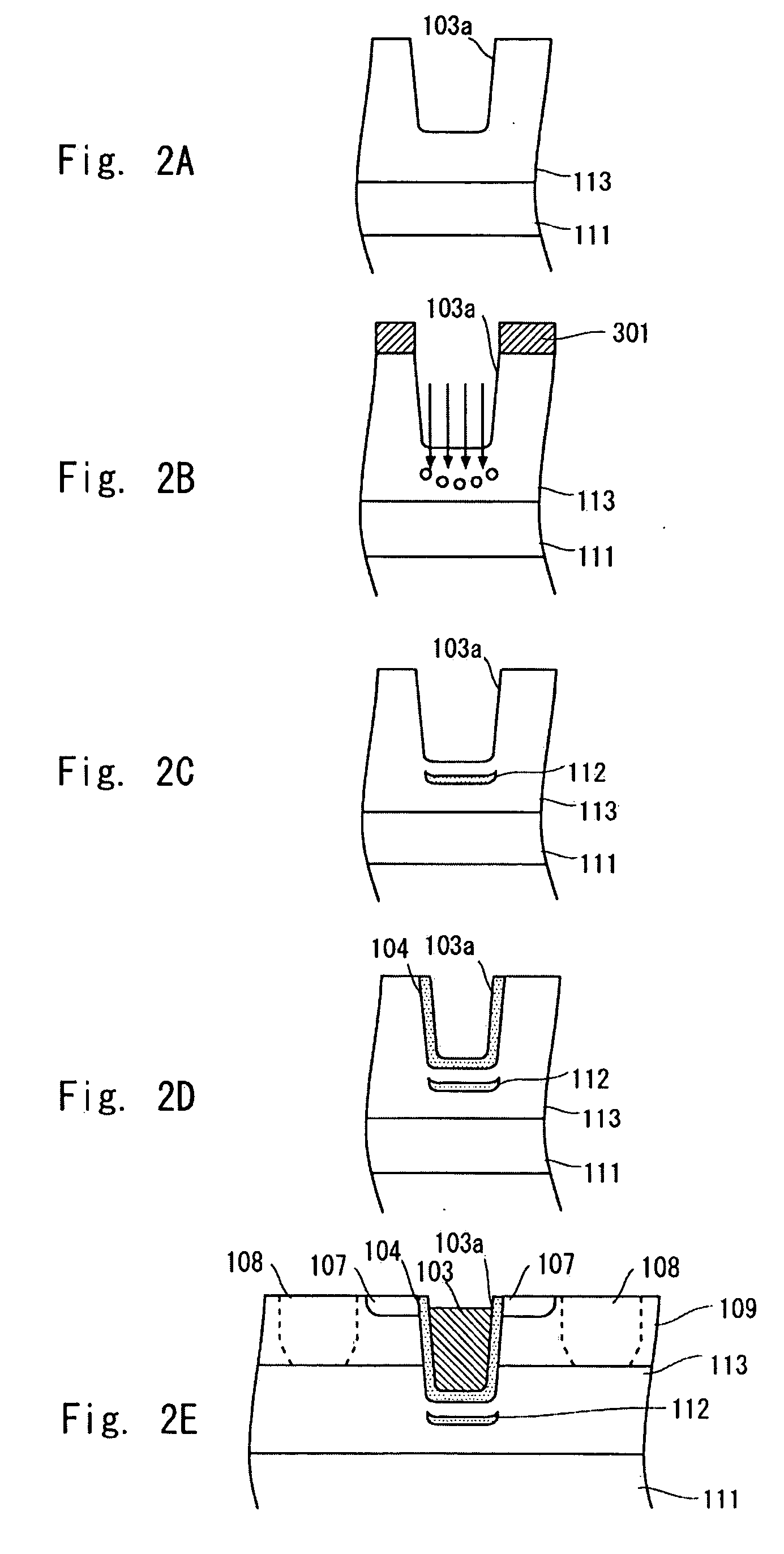
[0035] First, a semiconductor device according to a first embodiment of the present invention is described. The semiconductor device according to this embodiment has a feature that a buried oxide film is formed below a trench (gate electrode) away from a gate oxide film (trench bottom).

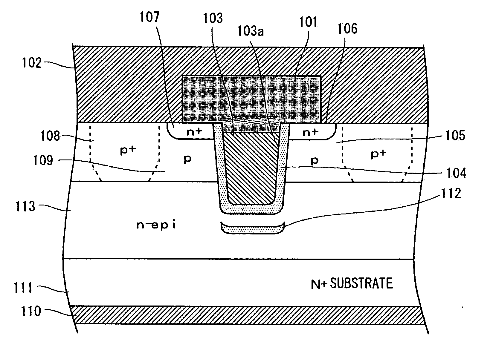
[0036]FIG. 1 is a sectional view of the semiconductor device according to this embodiment. This semiconductor device is a high-voltage vertical power MOSFET, in other words, a trench-gate type MOSFET.

[0037] As shown in FIG. 1, the semiconductor device includes a silicon substrate 111. The silicon substrate 111 is an n+ type (first conductivity type) semiconductor substrate having a high impurity concentration, for example. An epitaxial layer 113 is formed on the entire surface of the silicon substrate 111. The epitaxial layer 113 is an n− type semiconductor layer having an impurity concentration lower than the silicon substrate 111, for example. The epitaxial layer 113 forms a first semiconductor la...

second embodiment

[0058] Next, a semiconductor device according to a second embodiment of the present invention is described. The semiconductor device according to this embodiment has a feature that the number of buried oxide films as described in the first embodiment is increased.

[0059]FIG. 6 is a sectional view of the semiconductor device according to this embodiment. In FIG. 6, the same components as those of FIG. 1 are denoted by like reference numerals, and their description is omitted if not necessary. As shown in FIG. 6, the semiconductor device includes two buried oxide films 112 as compared with the structure of FIG. 1. In this example, the two buried oxide films 112 are arranged away from each other in parallel. As denoted by 301 of FIG. 6, the provision of the two buried oxide films 112 increases a proportion of the buried oxide film 112 to a region between the gate electrode 103 and the drain electrode 110. Thus, a gate capacitance can be made smaller than the first embodiment. For examp...


PUM


Abstract

To provide a semiconductor device capable of reducing a gate capacitance, and preventing breakdown of a gate oxide film if a large amount of current flows. A semiconductor device according to an embodiment of the present invention includes: an epitaxial layer; a channel region formed on the epitaxial layer; a trench extending from a surface of the channel region to the epitaxial layer; a gate oxide film that covers an inner surface of the trench; a gate electrode filled into the trench; and a buried insulating film formed below the gate electrode and away from the gate oxide film.

Description

BACKGROUND OF THE INVENTION [0001] 1. Field of the Invention [0002] The present invention relates to a semiconductor device and a manufacturing method for the same. In particular, the invention relates to a semiconductor device having a trench gate, and a manufacturing method for the same. [0003] 2. Description of Related Art [0004] Up to now, a vertical power MOSFET (Metal-Oxide Semiconductor Field Effect Transistor) has been known as a high-voltage MOSFET. In a trench-gate type MOSFET typifying such a power MOSFET, a gate electrode is provided inside a trench, and a channel region is formed in a vertical direction to easily shrink a cell pitch and realize a high degree of integration and a low on-resistance. However, a trench type MOSFET has a large gate capacitance (parasitic capacitance of a gate bottom portion), which leads to a great obstacle to the application to a high-speed switching element. Further, when a large amount of current (overcurrent) flows through the MOSFET, ch...

Claims


Application Information

Patent Timeline
Patent Type & Authority Applications(United States)
IPC IPC(8): H01L29/94
CPCH01L21/26533H01L29/0653H01L29/66734H01L29/7813H01L29/0873
Inventor KANEKO, ATSUSHI
Owner RENESAS ELECTRONICS CORP
Why Eureka
Try Eureka