Semiconductor chip

a technology of semiconductors and chips, applied in the field of semiconductor chips, can solve the problems of complex process and chipping of wafers, and achieve the effects of improving adhesiveness, simple procedures, and improving adhesiveness

Inactive Publication Date: 2006-09-21
RENESAS ELECTRONICS CORP
View PDF5 Cites 2 Cited by
  • Summary
  • Abstract
  • Description
  • Claims
  • Application Information

AI Technical Summary

Benefits of technology

[0032] According to the present invention, it is made possible to improve the adhesiveness between insulating materials of the semiconductor chip, by forming the stacked film on the semiconductor substrate and by supplying the oxidative gas during dicing. It is therefore no more necessary to carry out the plasma treatment every time the copper layer and the b...

Problems solved by technology

A problem has, however, arisen in that the interlayer insulating film composed of such low-dielectric-constant material is poor in adhesiveness with an etching stopper film typically made of SiCN or with a protective insulating film typically made of SiO2, which would result in peeling-off.
However, the individualization i...

Method used


Image

  • Semiconductor chip
  • Semiconductor chip
  • Semiconductor chip

Examples


first embodiment

(First Embodiment)

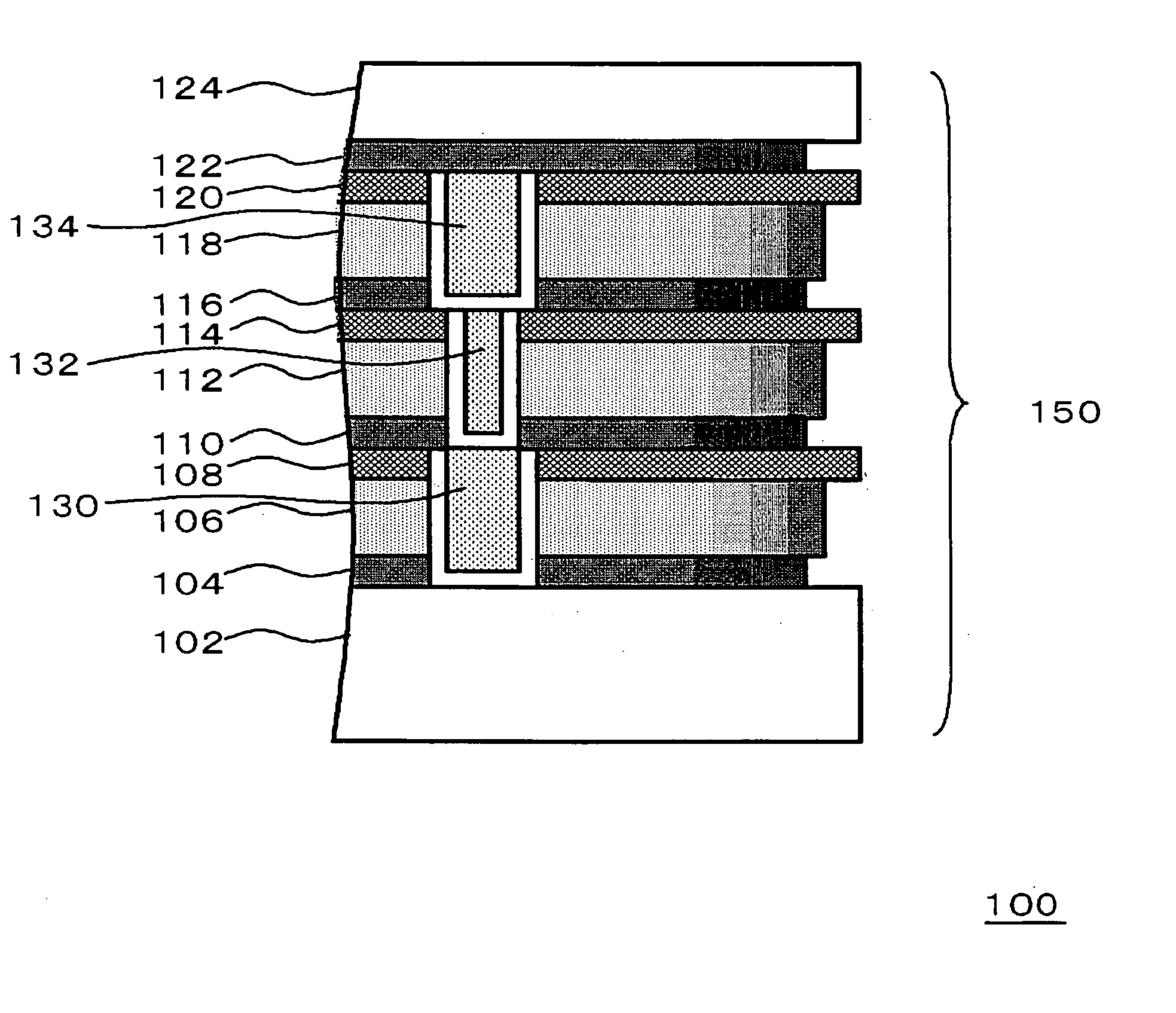
[0046]FIG. 1 is a sectional view showing a part of a configuration of the semiconductor chip of this embodiment.

[0047] The semiconductor chip 100 includes a semiconductor substrate (not shown) and a stacked film formed over the semiconductor substrate, which includes carbon-containing insulating films (a first interlayer insulating film 106, a second interlayer insulating film 112, a third interlayer insulating film 118, a first etching stopper film 104, a second etching stopper film 110, a third etching stopper film 116, and a fourth etching stopper film 122) and carbon-free insulating films (an underlying layer 102 including transistors, a top cover film 124, a first protective insulating film 108, a second protective insulating film 114, and a third protective insulating film 120). The end faces of the carbon-free insulating films herein are located on the outer side of the end faces of the carbon-containing insulating films.

[0048] The carbon-containing insula...

second embodiment

(Second Embodiment)

[0092] Also in this embodiment, the semiconductor chip has a configuration same as that of the semiconductor chip 100 of the first embodiment. This embodiment differs from the first embodiment in procedures of individualizing the semiconductor chips.

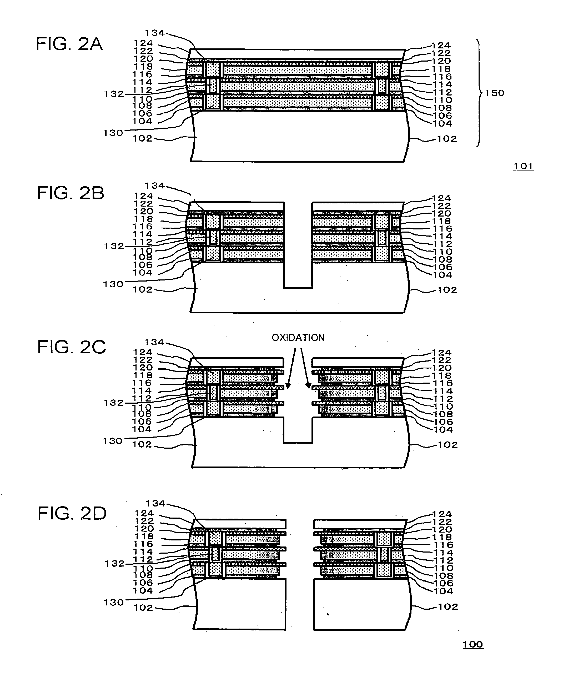
[0093]FIGS. 3A to 3C are sectional views showing process steps of fabricating the semiconductor chip 100 of this embodiment.

[0094] Also in this embodiment, the semiconductor device 101 is formed according to procedures similar to those in the first embodiment explained referring to FIG. 2A (FIG. 3A).

[0095] Then, firstly, the semiconductor device 101 is cut from the upper surface of the semiconductor substrate by blade dicing, laser dicing, or a combination of lithographic and etching techniques, along the outer periphery of the chips, to thereby individualize the semiconductor chips 100 (FIG. 3B). The side faces of the stacked film 150 are thus exposed. An oxidative gas is then supplied to the stacked film 150 havin...

third embodiment

(Third Embodiment)

[0097] Also in this embodiment, the semiconductor chip has a configuration same as that of the semiconductor chip 100 of the first embodiment. This embodiment differs from the first embodiment in procedures of individualizing and oxidizing the semiconductor chips.

[0098]FIGS. 4A to 4C are sectional views showing process steps of fabricating the semiconductor chip 100 of this embodiment.

[0099] Also in this embodiment, the semiconductor device 101 is formed according to procedures similar to those in the first embodiment explained referring to FIG. 2A (FIG. 4A). The semiconductor device 101 is then diced from the upper surface of the semiconductor substrate by blade dicing, laser dicing, or a combination of lithographic and etching techniques, along the outer periphery of the chips, and at the same time an oxidative gas is supplied so as to proceed oxidation (FIG. 4B). The side faces of the stacked film 150 of the semiconductor device 101 are thus oxidized. Conditio...


PUM


Abstract

A semiconductor chip 100 includes a semiconductor substrate (not shown), and a stacked film 150 formed over the semiconductor substrate, which includes carbon-containing insulating films such as a first interlayer insulating film 106, and carbon-free insulating films such as an underlying layer 102 and a top cover film 124. The end faces of the carbon-free insulating films herein are located on the outer side of the end faces of the carbon-containing insulating films. The carbon composition of the carbon-containing insulating films is lowered in the end portions thereof than in the inner portions. The film density of the carbon-containing insulating films is raised in the end portions thereof than in the inner portions.

Description

[0001] This application is based on Japanese patent application No. 2005-079105 the content of which is incorporated hereinto by reference. BACKGROUND [0002] 1. Technical Field [0003] The present invention relates to a technique of improving adhesiveness of a carbon-containing insulating film with other insulating films. [0004] 2. Related Art [0005] In keeping with recent demands on higher speed operations of semiconductor elements, extensive researches have been made on altering the interlayer insulating film in multi-level interconnect layers from conventional silicon oxide film (specific dielectric constant is approximately k=3.9) to a low-dielectric-constant material film, aiming at decreasing parasitic interconnect capacitance. The low-dielectric-constant material referred to herein means any insulating material having a specific dielectric constant of 3.3 or smaller. Carbon-containing silicon oxide material is one of such low-dielectric constant material, wherein recent invest...

Claims


Application Information

Patent Timeline
IPC IPC(8): H01L23/52
CPCH01L21/02126H01L21/02164H01L21/02167H01L21/022H01L21/02211H01L21/02274H01L21/02337H01L21/0234H01L21/02348H01L21/31633H01L21/78H01L23/5222H01L23/5329H01L23/53295H01L2924/0002H01L2924/00
Inventor OHTO, KOICHIUSAMI, TATSUYA
Owner RENESAS ELECTRONICS CORP
Why Eureka
Try Eureka