High frequency integrated circuit (hfic) microsystems assembly and method for fabricating the same

a microsystem and integrated circuit technology, applied in the direction of pulse technique, instrumentation, semiconductor/solid-state device details, etc., can solve the problems of complex infrastructure, difficult handling of pcbs, and packaging itself, and achieve cost-effective manufacturing, minimal transmission line loss, and improved interface

Active Publication Date: 2006-09-21
LOGICACMG WIRELESS NETWORKS
View PDF3 Cites 5 Cited by
  • Summary
  • Abstract
  • Description
  • Claims
  • Application Information

AI Technical Summary

Benefits of technology

[0005] It is therefor an object of the present invention to provide high frequency integrated circuit (HFIC) Microsystems assembly and methods for fabricating the same. Fabrication-wise fully planar approach creates an optimal HFIC-assembly that can be manufactured cost-effectively with minimal transmission line lossies. The approach makes further miniaturiazition of ICs possible: it improves interface between micro- and macroworlds by enabling remarkable red...

Problems solved by technology

Conventional electronic packaging has served the purpose of protecting electronic circuitry in low frequency applications while the package itself is the main cause of degradation in microwave applications.
Today packaging methods are very diversified and often the infrastructure is complex.
Until recently, EMS providers or packaging foundaries have packaged the ICs, while semiconductor industries have been providing the chips fabricated in clean rooms, where handling of PCBs is difficult.
Thereby, conventional partitioning of electronic packaging has presented a clear conflict in further miniaturiazition of HFICs that calls for improved interface between the...

Method used


Image

  • High frequency integrated circuit (hfic) microsystems assembly and method for fabricating the same
  • High frequency integrated circuit (hfic) microsystems assembly and method for fabricating the same
  • High frequency integrated circuit (hfic) microsystems assembly and method for fabricating the same

Examples


Embodiment Construction

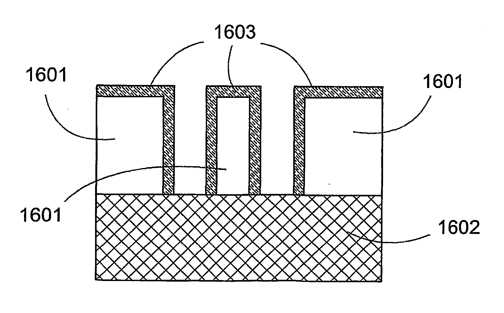
[0033] High frequency integrated circuit (HFIC) assembly may be used, e.g. in a conventional microwave package assembly or high performance subassembly in a printed circuit board (PCB) or it may itself form a PCB like structure, which eliminates most hazardous materials from the assembly process making it an environmentally friendly alternative for IC assembly purposes. This assembly may contain one or more chips and it can be single or multilevel structure.

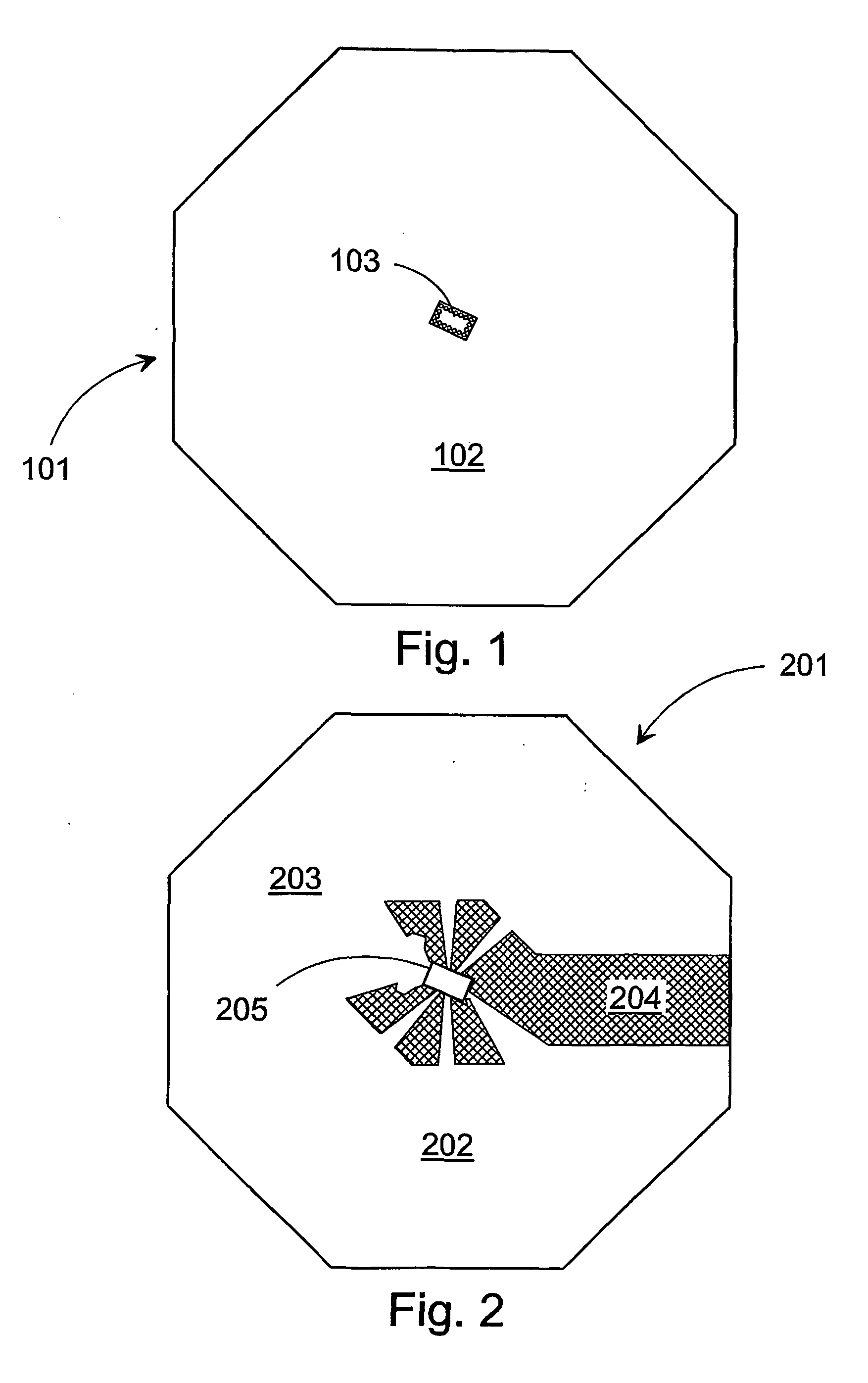
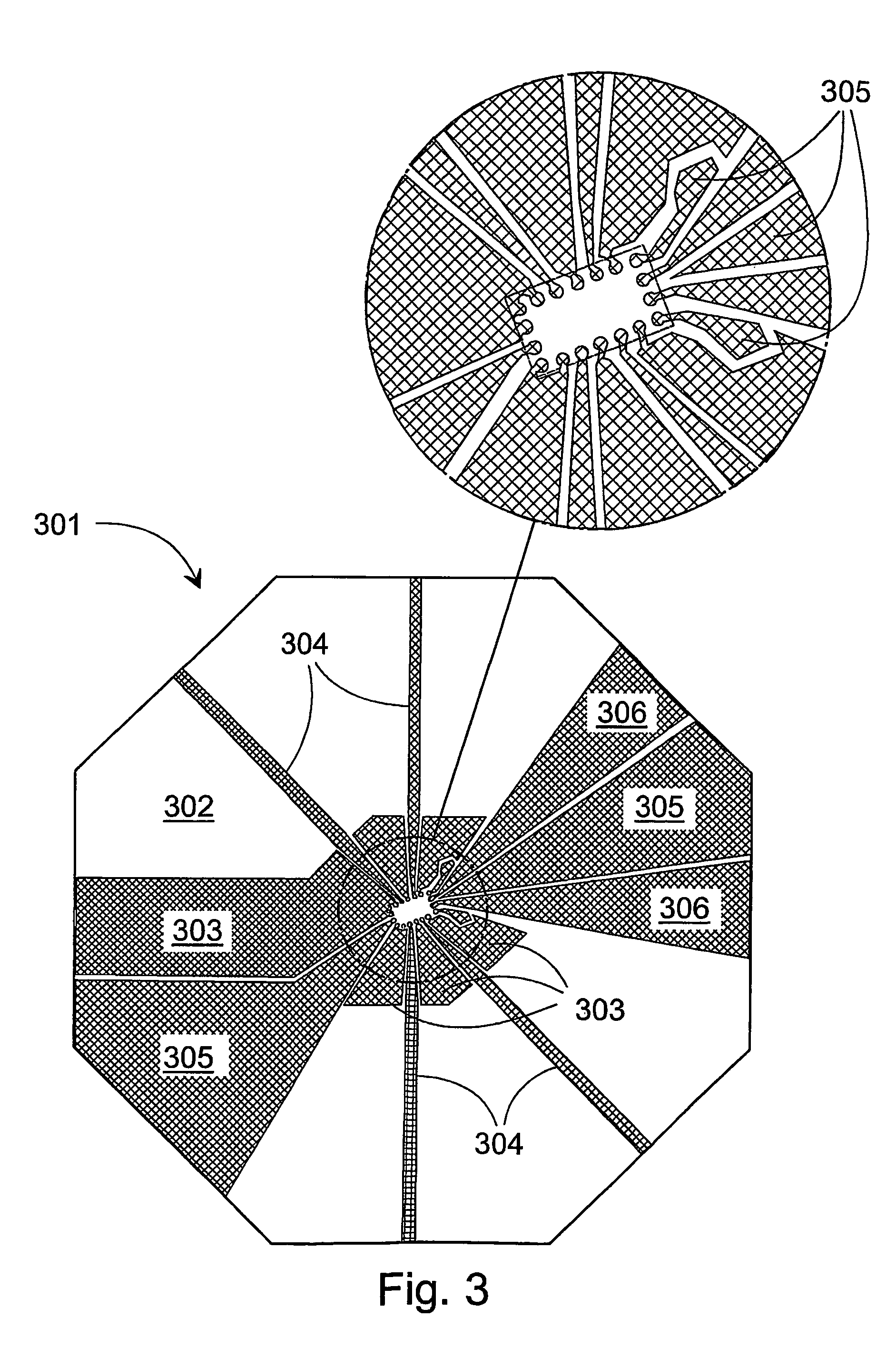
[0034]FIGS. 1 through 7 shows how one HFIC chip assembly can be formed and FIGS. 8 through 10 shows how HFIC assembly can be realized in a conventional microwave package structure, as a subassembly in a PCB board or can be realized as a PCB board itself.

[0035]FIGS. 1 through 3 presents main parts of the assembly, which contains a HFIC chip 103, the first substrate 201, the second substrate 301 and the third substrate 101. FIG. 1 shows the functional part 102 of the third substrate 101 and a HFIC chip 103. FIG. 2 shows the funct...


PUM

PropertyMeasurementUnit
Heightaaaaaaaaaa
Electrical conductivityaaaaaaaaaa
Electrical conductoraaaaaaaaaa

Abstract

High frequency integrated circuit (HFIC) microsystems assembly and method for fabricating the same are disclosed. Presented HFIC assembly method has the optimized structure for minimizing the losses in transmitting electronic and electromagnetic energy in interconnects; it optimizes the area used for interconnects and eliminates most hazardous materials from the assembly process making it an environmentally friendly alternative for IC assembly purposes. This versatile assembly process was developed specifically for HFIC packaging, but its versatility expands its usage from monolithic microwave integrated circuit (MMIC) packaging to partial PCB assemblies and due to environmental friendliness potentially replacing other PCB techniques especially in high performance applications. HFIC assembly comprises a first substrate (702, 703) and a second substrate (701) of conductor-on-insulator or similar having high aspect ratio trenches and conductors (705, 706, 707, 708) as well as a chip therebetween. A common ground (707, 708, 710, 710′, 711, 711′) formed by the first and second substrates encompass the chip at least adjacent the HF-signal paths (706).

Description

FIELD OF THE INVENTION [0001] This invention relates to high frequency integrated circuit (HFIC) Microsystems assembly comprising a substrate, a chip, signal paths for power and HF-signals and a grounding structure. Here high frequency is referred to broadband applications and, e.g., frequencies above five gigahertz (5 GHz), in particular. The invention deals also with the method for fabricating the same. BACKGROUND OF THE INVENTION [0002] The way microwave circuits, patterned metal traces on various microwave substrates, have commercially been packaged for over 30 years utilizing test fixtures and metal housings have to large extend remained the same. Conventional electronic packaging has served the purpose of protecting electronic circuitry in low frequency applications while the package itself is the main cause of degradation in microwave applications. Today, group IV circuits have reached ULSI era and group III-V ICs LSI / VLSI era. Early monolithic ICs brought about the requireme...

Claims


Application Information

Patent Timeline
IPC IPC(8): G01N30/86B81C1/00H01L21/58H01L23/12H01L21/60H01L23/13H01L23/14H01L23/498H01L23/552H01L23/66
CPCH01L23/057H01L2224/16227H01L23/147H01L23/49833H01L23/49838H01L23/552H01L23/66H01L2223/6627H01L2223/6688H01L2924/01078H01L2924/01079H01L2924/09701H01L2924/1423H01L2924/15153H01L2924/15162H01L2924/1517H01L2924/15173H01L2924/1903H01L2924/19033H01L2924/3025H01L2924/01087H01L2924/01029H01L2924/10253H01L23/13H01L2924/00H01L2224/16225
Inventor JUHOLA, TARJA A.
Owner LOGICACMG WIRELESS NETWORKS
Why Eureka
Try Eureka