Semiconductor composite apparatus, print head, and image forming apparatus

a technology of composite apparatus and print head, which is applied in the direction of semiconductor devices, semiconductor/solid-state device details, printing, etc., can solve the problems of inability to reduce the thickness of the chip further, uneconomical in terms of material utilization efficiency, and inability to achieve the reduction of manufacturing cost. , to achieve the effect of maintaining sufficient functions and performance and manufacturing at low cos

Inactive Publication Date: 2006-09-28
OKI DATA CORP
View PDF9 Cites 82 Cited by
  • Summary
  • Abstract
  • Description
  • Claims
  • Application Information

AI Technical Summary

Benefits of technology

[0011] An object of the invention is to provide a semiconductor composite apparatus that can be manufactured at low cost while maintaining sufficient functions and performance.

Problems solved by technology

This is uneconomical in terms of efficient utilization of material.
Thus, the thickness of the chips cannot be reduced any further as long as the chips are mounted on the unit substrate by the processes of dicing, picking-up, and bonding.
Thus, reduction of the manufacturing cost cannot be achieved by decreasing the thickness of the chip.

Method used


Image

  • Semiconductor composite apparatus, print head, and image forming apparatus
  • Semiconductor composite apparatus, print head, and image forming apparatus
  • Semiconductor composite apparatus, print head, and image forming apparatus

Examples


first embodiment

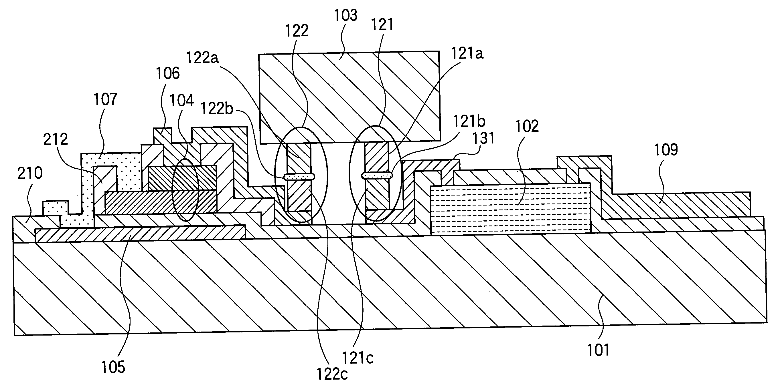
[0058] A semiconductor composite apparatus is a semiconductor thin film. High-speed circuits are formed of a single crystal semiconductor, which is expensive but is capable of fabricating high speed circuits that directly drive the active devices. Low-speed circuits are formed of a poly crystal semiconductor, which is inexpensive but is only capable of fabricating low speed circuits that control the high speed circuits. In other words, the functions of the semiconductor composite apparatus are apportioned into the high speed circuits and low speed circuits, thereby preventing the deterioration of functions as well as maintaining low manufacturing cost.

[0059] Large-current driving circuits are formed of a material capable of fabricating large-current circuits. Small-current driving circuits are formed of a material capable of only fabricating small-current circuits that drive the large-current driving circuits. In other words, the functions of the driving circuits are apportioned in...

second embodiment

[0083] In the first embodiment, the second driving circuits 103 are formed of the third semiconductor materials on a substrate. A second embodiment differs from the first embodiment in that the second driving circuits 103 are formed of the third semiconductor materials in a semiconductor thin film. Configurations similar to those in the first embodiment have been given the same reference numerals and their description is omitted.

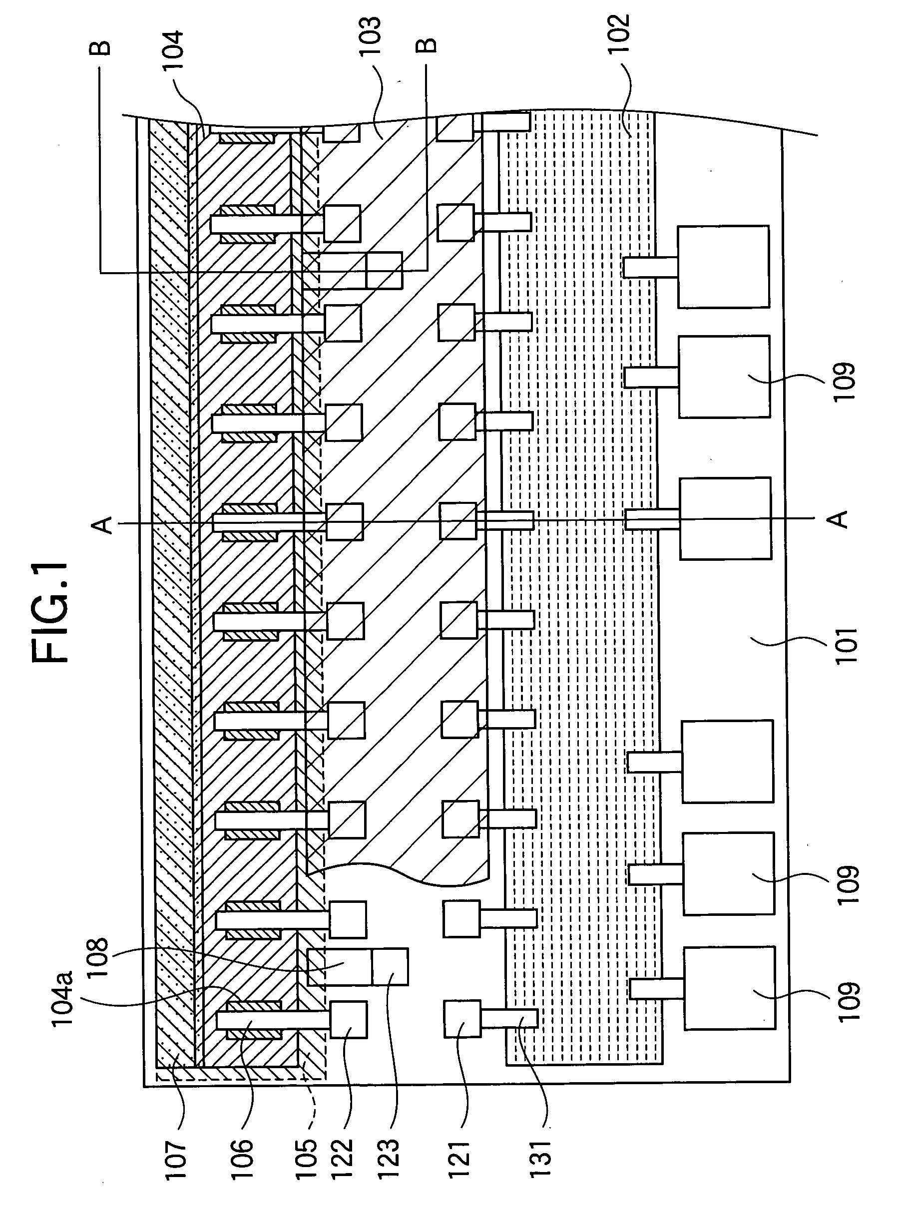
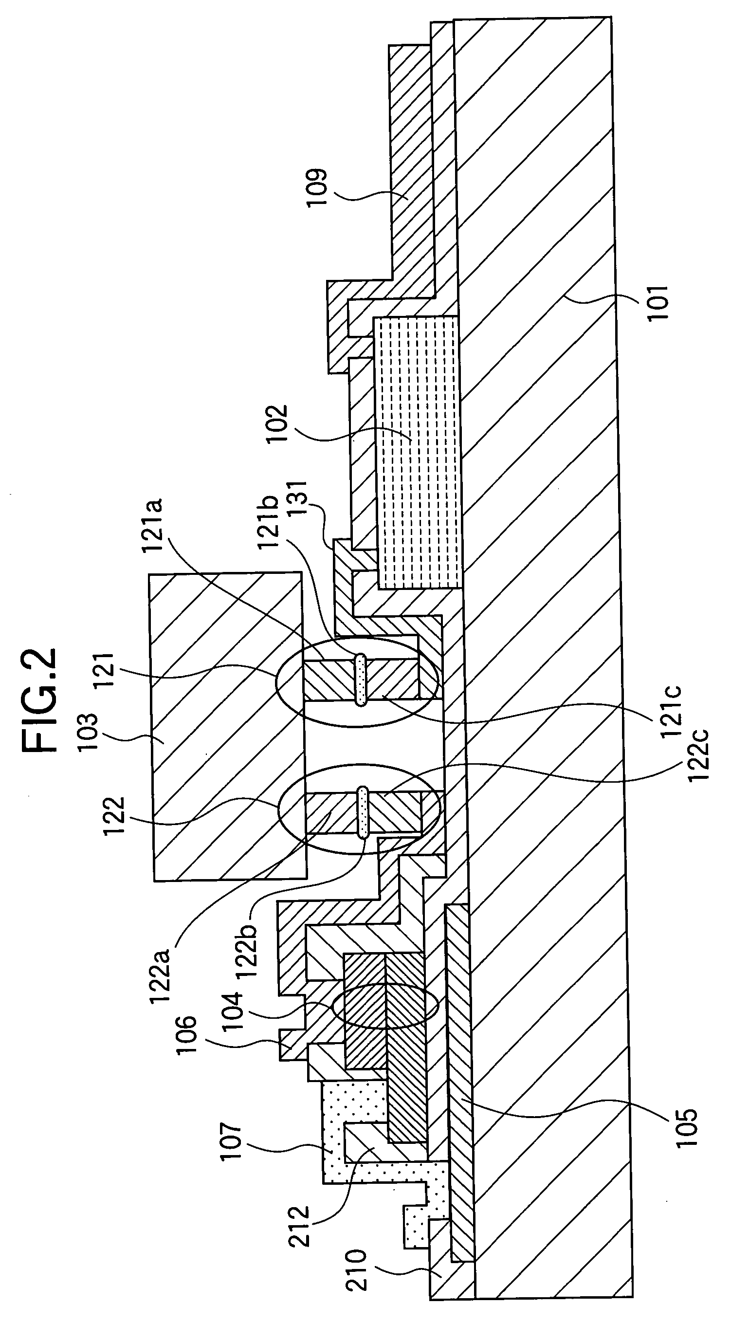
[0084]FIG. 7 is a top view illustrating a pertinent portion of the semiconductor composite apparatus. FIG. 8 is a cross sectional view taken along a line A-A of FIG. 7. FIG. 9 is a cross sectional view taken along a line B-B of FIG. 7. For better understanding of the structure, the interlayer dielectric film is omitted from FIG. 7.

[0085] In other words, the semiconductor composite apparatus includes first driving circuits 102 and the aforementioned semiconductor thin film layer 104 in the first embodiment, formed on the first substrate such as a glass subs...

third embodiment

[0090] A third embodiment differs from the first and second embodiments in the configuration of first driving circuits and second driving circuits. Elements similar to those in the first and second embodiments have been given the same reference numerals and their description is omitted.

[0091]FIG. 10 is a top view of a pertinent portion of a semiconductor composite apparatus according to the third embodiment. FIG. 11 is a cross sectional view taken along a line A-A of FIG. 10. FIG. 12 is a cross sectional view taken along a line B-B of FIG. 10. For better understanding of the embodiment, an interlayer dielectric film is omitted from FIG. 10. While the third embodiment will be described in terms of the semiconductor thin film layer 104 in the first embodiment, the semiconductor thin film layers 304 and 404 in the first embodiment may of course be used.

[0092] The second driving circuits 103 in the first embodiment and the second driving circuits 503 in the second embodiment are forme...


PUM


Abstract

A semiconductor composite apparatus, includes a first substrate, a semiconductor thin film layer, active devices, first driving circuits, and second driving circuits. The semiconductor thin film layer is formed on the first substrate and is formed of a first semiconductor material. The active devices are formed in the semiconductor thin film layer. The first driving circuits is formed of a second semiconductor material and performing a first function in which the active devices are driven. The second driving circuits are formed of a third semiconductor material and performing a second function in which the active devices are driven, the second function being different from the first function.

Description

BACKGROUND OF THE INVENTION [0001] 1. Field of the Invention [0002] The present invention relates to a semiconductor composite apparatus such as a light emitting diode (LED), a print head that uses such a semiconductor composite apparatus, and an image forming apparatus. [0003] 2. Description of the Related Art [0004] For example, Japanese Patent (Kokai) Publication No. 10-63807 discloses a conventional semiconductor composite apparatus in which light emitting elements and their driver circuits and semiconductor integrated circuits are fabricated. This semiconductor composite apparatus is a card type information-controlling apparatus that includes light-emitting / light-receiving elements and associated electronics on a substrate. The light-emitting / light-receiving elements are formed of semiconductor thin films, and convert electrical signals into light signals and light signals into electrical signals. The electronics includes semiconductor integrated circuit elements, capacitors, a...

Claims


Application Information

Patent Timeline
Patent Type & Authority Applications(United States)
IPC IPC(8): H01L23/34H01L33/08H01L33/10H01L33/30H01L33/58
CPCB41J2/45H01L25/167H01L2224/48091H01L2924/00014H01L2224/48464
Inventor OGIHARA, MITSUHIKOFUJIWARA, HIROYUKIMUTO, MASATAKASUZUKI, TAKAHITOIGARI, TOMOKI
Owner OKI DATA CORP
Why Eureka
Try Eureka