
Wiring board, electronic circuit board, electronic apparatus and manufacturing method of electronic circuit board

Inactive Publication Date: 2006-09-28
RICOH KK +1
View PDF17 Cites 9 Cited by
  • Summary
  • Abstract
  • Description
  • Claims
  • Application Information

AI Technical Summary

Benefits of technology

[0033] Accordingly, it is a general object of the present invention to provide a novel and useful wiring board, electronic circuit board, electronic apparatus and manufacturing method of the electronic circuit board, in which one or more of the problems described above are eliminated.
[0034] More specifically, a first object of an embodiment of the present invention is to provide a wiring board whereby fragility of solder due to a great amount of gold formed on an electrode surface of the wiring board in the solder can be avoided and a part of plural electrodes can work well as a contact electrode.
[0035] A second object of the embodiment of the present invention is to provide wiring board manufactured at low cost by being so made as to be kept.
[0036] A third object of the embodiment of the present invention is to provide an electronic circuit board and a manufacturing method of the electronic circuit board, whereby in the electronic circuit board signal transmission speed between electronic parts can be made high and noise mixture can be reduced.
[0037] A fourth object of the embodiment of the present invention is to provide an electronic circuit board and a manufacturing method of the electronic circuit board, whereby an underfill process of a small size electronic part can be easily done.

Problems solved by technology

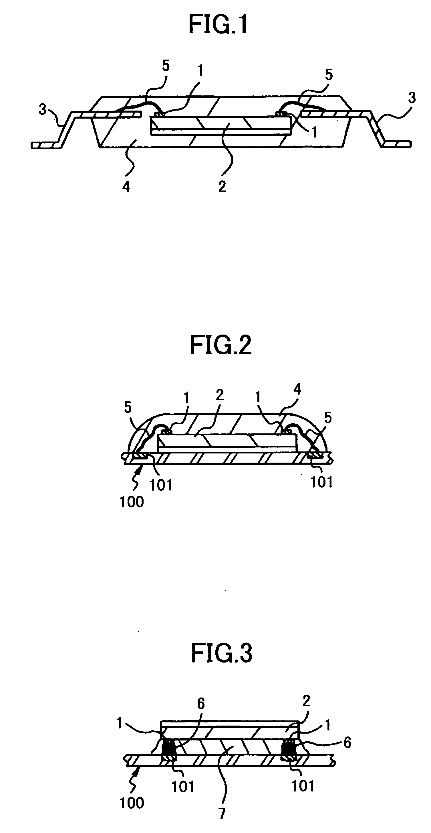
Since the metal mother material covered with the oxide film repels the molten solder, it is difficult to implement good solder connections.
However, in this method, a great number of the wiring boards 100 so made cannot be kept.
If the amount of the educed gold is too much, the solder 6 after being solidifying becomes extremely fragile.
In an electrolytic plating process, since the thickness of the Au surface layer may be approximately 2 μm, it is not possible to prevent the solder 6 from becoming fragile.
However, in such a wiring board 100, some of the plural electrodes 101 formed on the wiring board 100 cannot work well as contact electrodes.
However, there is no discussion about a technique whereby the signal transmission speed between electronic parts can be made high and noise mixture can be reduced, in Japanese Laid-Open Patent Application Publications No. 2001-308268 or No. 2003-282630.
In the manufacturing method of the electronic circuit board discussed in Japanese Laid-Open Patent Application Publications No. 2001-308268 and No. 2003-282630, depending on the structure of the bare chip 2, the underfill process may be difficult.
However, if this opening is too small, sufficient capillary action cannot be obtained and therefore the underfill process may be difficult.

Method used


Image

  • Wiring board, electronic circuit board, electronic apparatus and manufacturing method of electronic circuit board
  • Wiring board, electronic circuit board, electronic apparatus and manufacturing method of electronic circuit board
  • Wiring board, electronic circuit board, electronic apparatus and manufacturing method of electronic circuit board

Examples


Embodiment Construction

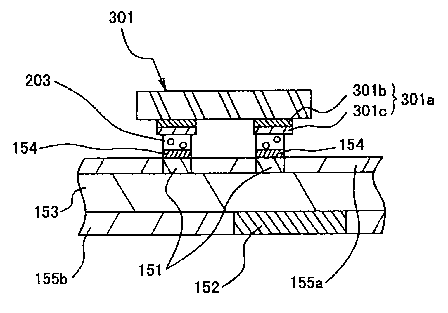
[0066] A description of the present invention and details of drawbacks of the related art are now given, with reference to FIG. 6 through FIG. 24, including embodiments of the present invention.

[0067] More specifically, embodiments of a Printed Wiring Board (PWB) as a wiring board of the present invention, a module board as an electronic circuit board of the present invention, and a manufacturing method of the electronic circuit board are discussed.

[0068] First, the embodiment of the Printed Wiring Board (PWB) as the wiring board of the present invention is discussed.

[0069]FIG. 6 is a plan view seen from a first surface side of a Printed Wiring Board (PWB) 150.

[0070] An electrode pattern of plural non-Au electrodes 151 is formed on a first surface of the PWB 150 by a well-known technique. The first surface includes an electrode block mounting area R1, Surface Mount Device (SMD) mounting area R2, and a flip chip mounting area R3.

[0071] The electrode block mounting area R1 is whe...


PUM


Abstract

A wiring board includes a substrate made of an insulation material and wired by a conductive material. A plurality of electrodes is formed on a surface of the substrate. A non-Au electrode not having an Au surface layer and an Au electrode having the Au surface layer are formed as the electrodes.

Description

CROSS-REFERENCE TO RELATED APPLICATION [0001] This application is a U.S. continuation application filed under 35 USC 111(a) claiming benefit under 35 USC 120 and 365(c) of PCT application JP2005 / 14748, filed Aug. 11, 2005, which claims priority to Applications Ser. No. 2004-235438 filed in Japan on Aug. 12, 2004, No. 2004-235448 filed in Japan on Aug. 12, 2004, and No. 2005-215800 filed in Japan on Jul. 26, 2005. The foregoing applications are hereby incorporated herein by reference. BACKGROUND OF THE INVENTION [0002] 1. Field of the Invention [0003] The present invention relates to a wiring board such as a printed wiring board where plural electrodes are formed on a surface of a substrate made of an insulation material for mounting an electronic part such as IC chip or a condenser, an electronic circuit board, an electronic apparatus and a manufacturing method of the electronic circuit board. [0004] 2. Description of the Related Art [0005] Conventionally, electronic circuit boards,...

Claims


Application Information

Patent Timeline
IPC IPC(8): H01L23/48
CPCH01L21/4867H01L21/563H01L23/498H01L23/49894H01L24/45H01L24/48H01L24/81H01L2224/05624H01L2224/05644H01L2224/05647H01L2224/1147H01L2224/13144H01L2224/16225H01L2224/32225H01L2224/45144H01L2224/48091H01L2224/48227H01L2224/48247H01L2224/48465H01L2224/73203H01L2224/73204H01L2224/73265H01L2224/81193H01L2224/8121H01L2224/81815H01L2224/83102H01L2224/92125H01L2924/01002H01L2924/01003H01L2924/01004H01L2924/01013H01L2924/01014H01L2924/01018H01L2924/01028H01L2924/01029H01L2924/01033H01L2924/0105H01L2924/01078H01L2924/01079H01L2924/01082H01L2924/014H01L2924/14H01L2924/19041H01L2924/19105H01L2924/3011H05K1/0268H05K3/243H05K3/282H05K3/328H05K3/341H05K2201/0352H05K2201/0391H05K2201/10674H05K2203/162H01L24/32H01L2924/01006H01L2224/48799H01L2224/45147H01L2224/48624H01L2224/48644H01L2224/48647H01L2224/81024H01L2224/32245H01L2224/81192H01L2224/0401H01L2924/00014H01L2924/00H01L2924/3512H01L2924/00012H01L2924/00011H01L2924/12042H01L24/73H01L2924/181H01L2924/00015H01L2224/43H01L2224/43848
Inventor MORIYAMA, EIJI
Owner RICOH KK
Learn More