Manufacturing method for semiconductor device, semiconductor device, and electronic apparatus

a manufacturing method and semiconductor technology, applied in semiconductor devices, semiconductor/solid-state device details, electrical apparatus, etc., can solve the problems of system lsi not maintaining the recent development cycle of electronic apparatus, limiting downsizing packaging, and long wiring lengths, so as to increase the bonding surface area, increase the reliability of three-dimensional packaging structure, and increase the bonding strength

Active Publication Date: 2006-09-28
SAMSUNG ELECTRONICS CO LTD
View PDF12 Cites 12 Cited by
  • Summary
  • Abstract
  • Description
  • Claims
  • Application Information

AI Technical Summary

Benefits of technology

[0013] According to this aspect, hole portions whose entire width is substantially identical to the width of the opening are formed on a part of the active surface side of the substrate, a curved surface is formed on the bottom surface of the hole portions while the width of the bottom surface of the hole portion is maintained substantially identical to the width of the opening, a connecting terminal is formed by burying metal in a hole portion, processing of the back surface of the substrate is carried out to expose a part of a connecting terminal, and thereby the distal end of an exposed connecting terminal has imparted the shape of the curved surface that has been formed at the hole portion. Thereby, it is possible to increase the bonding strength during bonding by increasing the bonding surface area of this connecting terminal, and it is possible to guarantee a high reliability. In addition, when a curved surface has been imparted to the bottom surface, the width of the bottom surface is maintained substantially identical to the width of the opening, and thereby it is possible to use the present invention even in the case that the connecting terminals are arranged at a narrow pitch without the distal end of a connecting terminal becoming greatly larger than the width of the opening.
[0043] According to this invention, the semiconductor devices are stacked in plurality on the mounting substrate and the connecting terminals having an increased bonding surface area are bonded together or the connecting terminals having the increased bonding surface area and the mounting substrate are bonded, and thereby it is possible to increase the bonding strength and it is possible to increase the reliability of the three-dimensional packaging structure.

Problems solved by technology

In the current situation, system LSI has failed to maintain the recent development cycle of electronic apparatus.
Conventionally, the electrodes formed on each IC are electrically connected by using a wire bonding technology, but in connections by wire bonding, the wiring length becomes long, and thus there is a limit to downsizing the packaging.
However, in the case that the electrical component is mounted in a portable electrical device, it is necessary to guarantee a higher strength because it can be anticipated that strong vibrations and shocks will be received from the outside.
Thus, the bonding between the connecting terminals of the stacked chips is two-dimensional, and there is the problem that the bonding strength is low, and thereby the reliability is low.

Method used


Image

  • Manufacturing method for semiconductor device, semiconductor device, and electronic apparatus
  • Manufacturing method for semiconductor device, semiconductor device, and electronic apparatus
  • Manufacturing method for semiconductor device, semiconductor device, and electronic apparatus

Examples


first embodiment

[0065] The Manufacturing Method for a Semiconductor Device

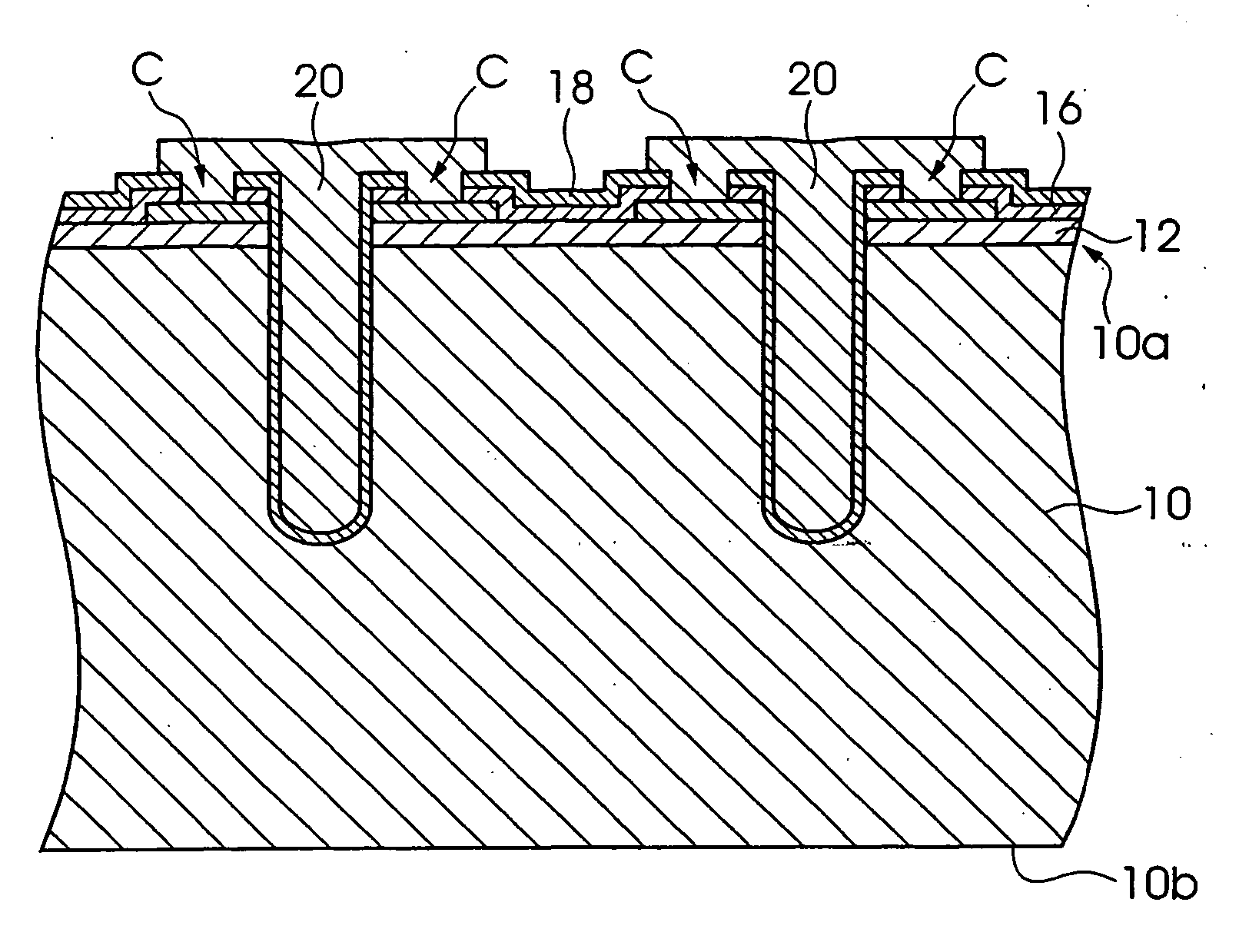
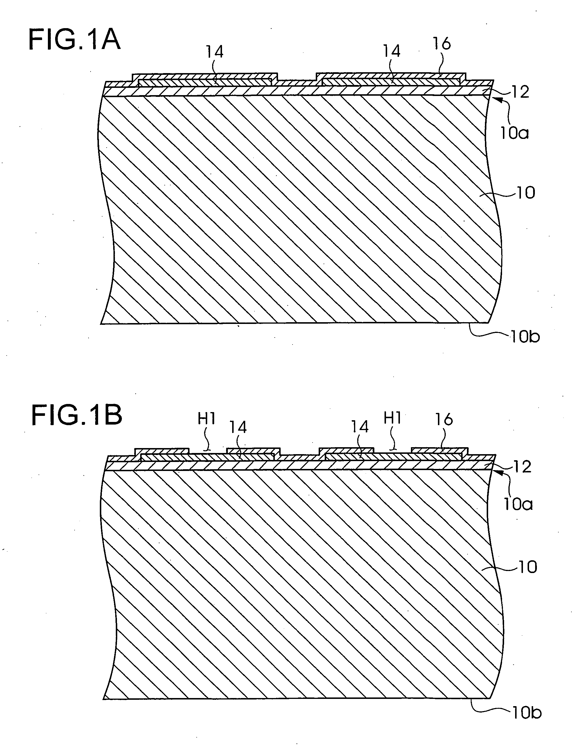
[0066]FIG. 1A to FIG. 6 are process drawings showing the manufacturing method for a semiconductor device according to a first embodiment of the present invention. FIG. 1A is a cross sectional drawing showing a part of the substrate, which is the processing object, in the wafer state. The substrate 10 is, for example, an Si (silicon) substrate, and on the active surface 10a side thereof, electronic elements consisting of transistors, memory elements other electric elements, along with electrical wiring (not illustrated), and electrode pads 14 that serve as the external electrodes of the electronic circuit, are formed. In contrast, on the back surface 10b of the substrate 10, these electronic circuits are not formed. The thickness of the substrate 10 is approximately 500 μm.

[0067] As shown in FIG. 1A, on the substrate 10, an insulating film 12 is formed by forming in sequence an insulating film consisting of an oxide film (SiO...

second embodiment

[0105] Manufacturing method for a semiconductor device

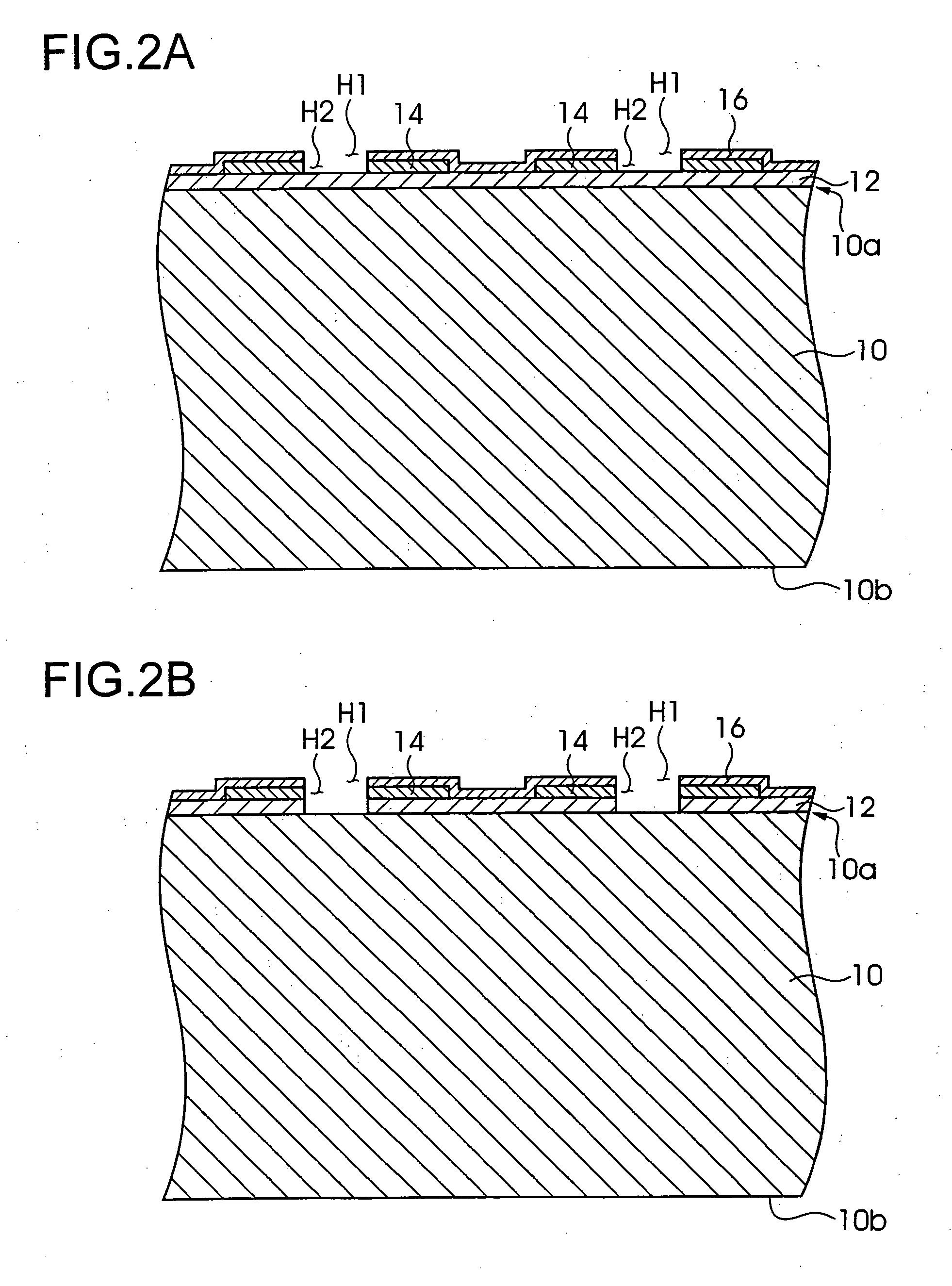
[0106]FIG. 7 to FIG. 12 is a step diagram showing a manufacturing method for a semiconductor device according to a second embodiment of the present invention. In this embodiment as well, first, using the substrate 10 having the structure formed in FIG. 1A, the opening of the passivation film 16, the opening of the electrode pads 14, and the opening of the insulating film 12 are carried out in sequence, and as shown in FIG. 2B, the exposing of a part of the substrate 10 is identical to that of the first embodiment.

[0107] In the present embodiment, in the opening portions H1 and H2 that expose a part of the substrate 10, which has the shape shown in FIG. 2B, masks having a predetermined shape are formed. FIG. 7A is a cross-sectional drawing showing the state in which masks have been formed in the opening portions H1 and H2, and FIG. 7B is an a drawing of the top surface showing an example of the masks. The masks 30 formed inside t...

third embodiment

[0124] Manufacturing method for a semiconductor device

[0125]FIG. 13 to FIG. 17 are step diagrams showing the manufacturing method for a semiconductor device according to a third embodiment of the present invention. In the present embodiment as well, first, using a substrate 10 having the structure shown in FIG. 1A, the opening of the passivation film 16, the opening of the electrode pads 14, and the opening of the insulating film 12 are carried out in sequence, and as shown in FIG. 2B, the exposing of a part of the substrate 10 is identical to that in the first embodiment.

[0126] In the present embodiment, the insulating film 40 consisting of SiO2 or the like is formed on the passivation film 16, including the opening portions H1 and H2, from which a part of the substrate in the state shown in FIG. 2B is exposed, and the insulating film 40 formed in the opening portions H1 and H2 is patterned into a predetermined shape (mask formation step). FIG. 13A is a drawing showing the state i...


PUM


Abstract

A manufacturing method for a semiconductor device includes a hole portion formation step for forming hole portions whose entire width is substantially identical to the width of the opening portion in a part of the active surface side of the substrate on which electronic components are formed, a curved surface formation step for curving the bottom surface of the hole portion while maintaining the width of the bottom surface in the hole portions substantially identical to the width of the opening portion, a connecting terminal formation step for forming connecting terminals that serve as the external electrodes of the electronic circuits by burying metal in the hole portions, and an exposure step for exposing a part of the connecting terminals by carrying out processing on the back surface of the substrate.

Description

CROSS REFERENCE TO RELATED APPLICATIONS [0001] This application is a divisional patent application of U.S. Ser. No. 10 / 774,362 filed Feb. 6, 2004, claiming priority to Japanese Patent Application No. 2003-082965 filed Mar. 25, 2003, which is incorporated herein by reference.BACKGROUND OF THE INVENTION [0002] 1. Field of the Invention [0003] The present invention relates to a manufacturing method for a semiconductor device, to a semiconductor device made thereby, and to an electronic apparatus provided with the semiconductor device. [0004] 2. Description of Related Art [0005] Presently, due to the implementation of downsizing and weight reduction in portable electronic apparatus such as notebook computers, PDAs (Personal Data Assistants) and the like, and devices such as sensors, micromachines, and heads for printers, research and development related to downsizing various types of electronic components such as the semiconductor chips provided therein is flourishing. In addition, in o...

Claims


Application Information

Patent Timeline
Patent Type & Authority Applications(United States)
IPC IPC(8): H01L23/52H01L23/12H01L23/04H01L21/306H01L21/3065H01L21/308H01L21/3205H01L21/60H01L21/768H01L23/48H01L25/065H01L25/07H01L25/18
CPCH01L21/30604H01L21/3065H01L21/3083H01L21/76898H01L23/481H01L25/0657H01L2225/06541H01L2224/03H01L2224/13147H01L2924/00014H01L2224/81815H01L2224/131H01L2924/014H01L24/03H01L24/05H01L24/11H01L24/13H01L24/81H01L2224/13009H01L2224/13019H01L2224/13025H01L2224/16146H01L2224/81193H01L2224/94H01L2224/11H01L2924/181H01L2224/0401H01L2924/14H01L2924/00
Inventor MATSUO, YOSHIHIDE
Owner SAMSUNG ELECTRONICS CO LTD
Why Eureka
Try Eureka