Pattern exposure method and apparatus

a pattern exposure and apparatus technology, applied in the direction of polarising elements, printing, instruments, etc., can solve the problems of increasing the cost and delay of the date of delivery, difficult to eliminate design errors perfectly, and shortening the time allotted to design and production of these substrates, so as to improve the exposure efficiency of solder resist and efficient maskless exposure

Inactive Publication Date: 2006-09-28
HITACHI SEIKO LTD
View PDF11 Cites 11 Cited by
  • Summary
  • Abstract
  • Description
  • Claims
  • Application Information

AI Technical Summary

Benefits of technology

[0014] Maskless exposure can be performed efficiently with high-directivity illumination light. In addition, the exposure efficiency of solder resist can be improved.

Problems solved by technology

In recent years, in spite of requiring more large-sized substrates, the time allotted to design and production of these substrates becomes shorter and shorter.
When the substrates are designed, it is very difficult to eliminate design errors perfectly.
A mask produced for each of many kinds of substrates results in increase of the cost and delay of the date of delivery.
However, according to the first method, the apparatus cost increases, and the running cost increases.
On the other hand, according to the second method, it is difficult to pattern a large area with high definition.
Thus, the apparatus cost increases, and the running cost increases.
However, it is difficult to obtain high-directivity exposure illumination light efficiently from the mercy lamp.

Method used


Image

  • Pattern exposure method and apparatus
  • Pattern exposure method and apparatus
  • Pattern exposure method and apparatus

Examples


first embodiment

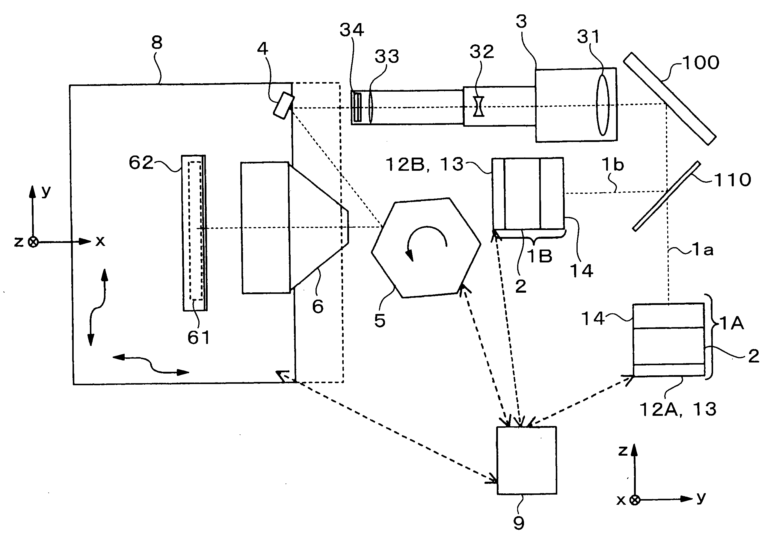
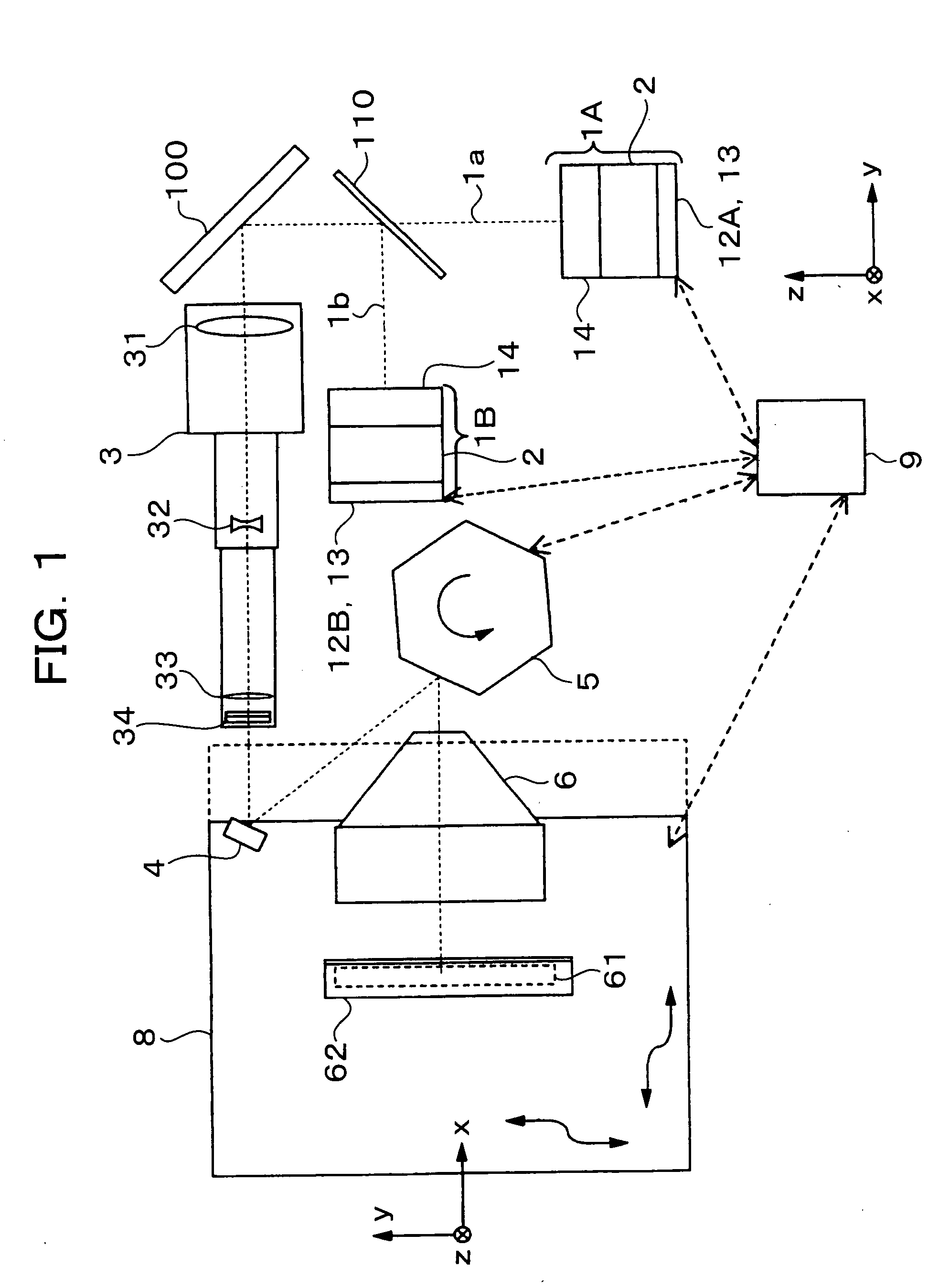
[0026]FIG. 1 is a configuration diagram of a maskless exposure apparatus according to a first embodiment of the present invention.

[0027] A light source optical system 1A is constituted by a plurality of (128 in this embodiment) blue-violet semiconductor lasers 12A and so on for outputting laser beams with a wavelength of 405 nm. The blue-violet semiconductor lasers 12A output 128 laser beams 1a. There is a variation of 405±7 nm in the wavelength of the laser beams 1a output from the blue-violet semiconductor lasers 12A.

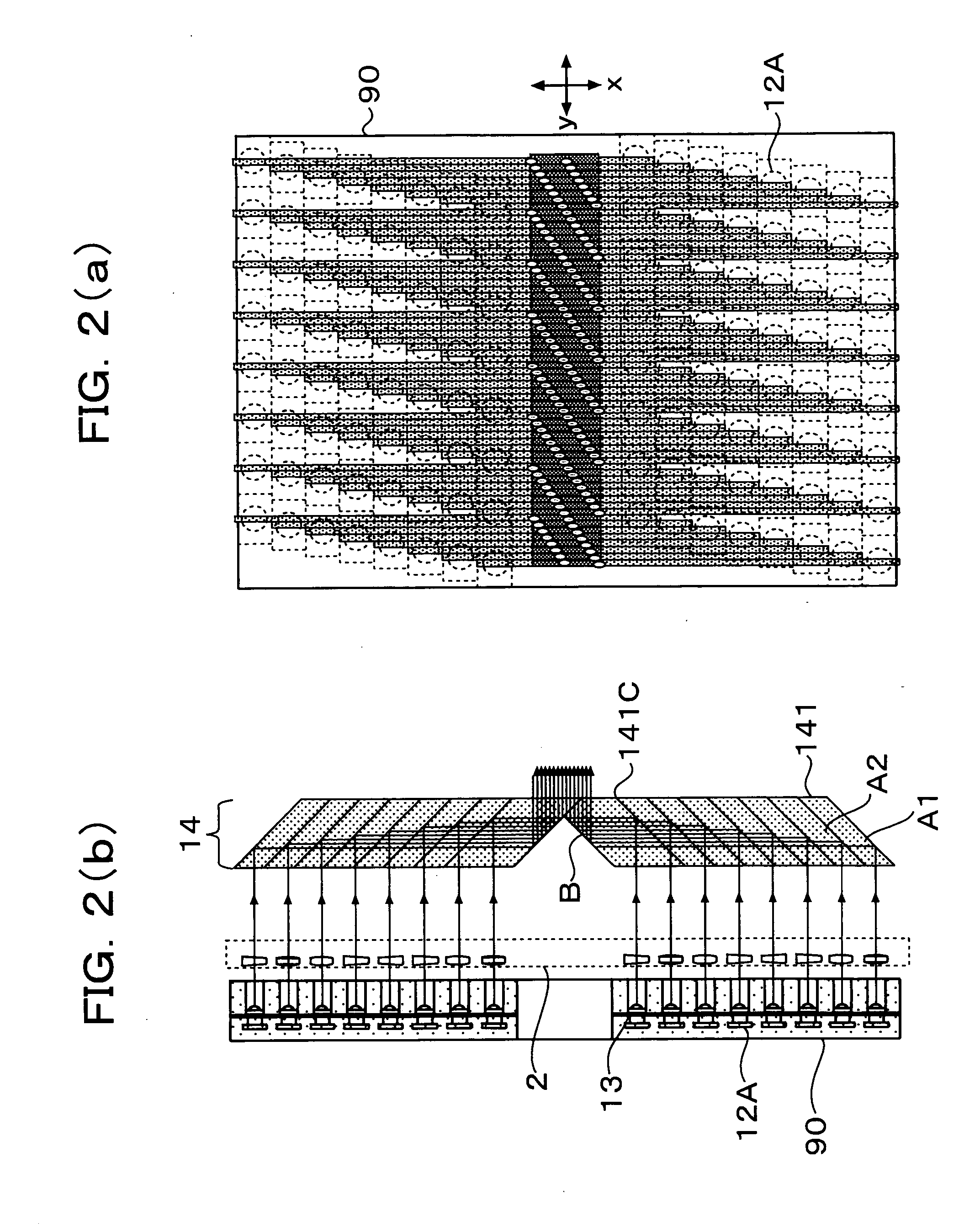
[0028] Next, the light source optical system 1A will be described in more detail with reference to FIGS. 2A and 2B.

[0029]FIGS. 2A and 2B are configuration views of the light source optical system 1A. FIG. 2A is a view viewed from the traveling direction of the laser beams 1a. FIG. 2B is a view viewed from a direction where the traveling direction of the laser beams 1a is parallel to the paper.

[0030] The light source optical system 1A is constituted by 128 blue-vio...

second embodiment

[0064]FIG. 7 is a configuration diagram of a maskless exposure apparatus according to a second embodiment of the present invention. FIGS. 8A and 8B are configuration views of a light source optical system 1C. FIG. 8A is a view viewed from a traveling direction of laser beams. FIG. 8B is a view viewed from a direction where the traveling direction of the laser beams is parallel with the paper. Parts the same as or functionally the same as those in FIGS. 1 and 2A-2B are referenced correspondingly, and so the description thereof will be omitted.

[0065] In the aforementioned first embodiment, only the blue-violet semiconductor lasers 12A or the ultraviolet semiconductor lasers 12B are held on one semiconductor laser holder substrate 90. In the second embodiment, however, 80 blue-violet semiconductor lasers 12A (designated by the white circles in FIGS. 8A-8B) and 48 ultraviolet semiconductor lasers 12B (designated by the shaded circles in FIGS. 8A-8B) are mixed and held on one semiconduc...

third embodiment 3

[0070]FIG. 9 is a configuration diagram of a maskless exposure apparatus according to a third embodiment of the present invention. Parts the same as or functionally the same as those in FIGS. 1 and 2A-2B are referenced correspondingly, and so the description thereof will be omitted.

[0071] A high-power infrared semiconductor laser is mounted inside an infrared light source 7. One end of an optical fiber 71 consisting of a bundle of plural fibers is connected to the infrared light source 7. The other end portion 72 of the optical fiber 71 has a configuration in which the plural fibers are arranged to be long laterally (for example, in a single horizontal line). The other end portion 72 is positioned in a position facing a region to be scanned with a polygon mirror 5.

[0072] Due to the aforementioned configuration, infrared light emitted from the semiconductor laser inside the infrared light source 7 enters the optical fiber 71 and leaves the optical fiber 71 from the outgoing end sur...


PUM


Abstract

A maskless exposure method and a maskless exposure apparatus in which maskless exposure can be performed efficiently with high-directivity illumination light, while the exposure efficiency of solder resist can be improved. Blue-violet semiconductor lasers 12A emitting laser beams 1a with a wavelength of 405 nm and ultraviolet semiconductor lasers 12B emitting laser beams 1b with a wavelength of 375 nm are provided to irradiate a substrate 8 with the laser beams 1a and 1b whose optical axes are made coaxial. In this event, one and the same place on the substrate 8 is irradiated with the laser beams 1a and 1b a plurality of times. Thus, the variation in intensity of the laser beams 1a and 1b is averaged.

Description

FIELD OF THE INVENTION [0001] The present invention relates to a pattern exposure method and a pattern exposure apparatus in which laser beams are converged on a substrate to be exposed, so as to scan the substrate and draw a pattern, and particularly relates to a pattern exposure method and a pattern exposure apparatus in which a substrate is irradiated with a plurality of laser beams output from a plurality of lasers so as to expose a plurality of portions of the substrate simultaneously. DESCRIPTION OF THE BACKGROUND ART [0002] In the background art, for exposing pattern on a printed circuit board, a TFT substrate or a color filter substrate of a liquid crystal display or a substrate of a plasma display (hereinafter referred to as “substrate” simply), a mask serving as a pattern master is produced, and the substrate is exposed with the mask in a mask exposure apparatus. [0003] In recent years, in spite of requiring more large-sized substrates, the time allotted to design and prod...

Claims


Application Information

Patent Timeline
Patent Type & Authority Applications(United States)
IPC IPC(8): G03B27/52
CPCG02B26/12G02B26/123G03F7/70383G03F7/70466G03F7/70575G03F7/70791G02C5/008G02C5/143G02C5/16G02C5/20
Inventor OSHIDA, YOSHITADANAITO, YOSHITATSUSUZUKI, MITUHIROYAMAGUCHI, TSUYOSHIMARUYAMA, SHIGENOBU
Owner HITACHI SEIKO LTD
Why Eureka
Try Eureka