Capacitive coupling plasma processing apparatus and method for using the same

a plasma processing and capacitive coupling technology, applied in the direction of coatings, electric discharge lamps, electric lighting sources, etc., can solve the problems of energy loss and excessive consumption of rf power as joule heat, and achieve the effect of high plasma uniformity

Active Publication Date: 2006-10-05
TOKYO ELECTRON LTD
View PDF7 Cites 230 Cited by
  • Summary
  • Abstract
  • Description
  • Claims
  • Application Information

AI Technical Summary

Benefits of technology

[0012] An object of the present invention is to provide a plasma processing apparatus of the capacitive coupling type and a method for using the same, which can easily attain high plasma uniformity. Another object of the present invention is to provide a plasma processing apparatus of the capacitive coupling type and a method for using the same, which can attain an arbitrary plasma distribution.

Problems solved by technology

However, the structure according to the technique disclosed in Patent Document 2 may consume too much RF power as Joule heat (energy loss).

Method used


Image

  • Capacitive coupling plasma processing apparatus and method for using the same
  • Capacitive coupling plasma processing apparatus and method for using the same
  • Capacitive coupling plasma processing apparatus and method for using the same

Examples


first embodiment

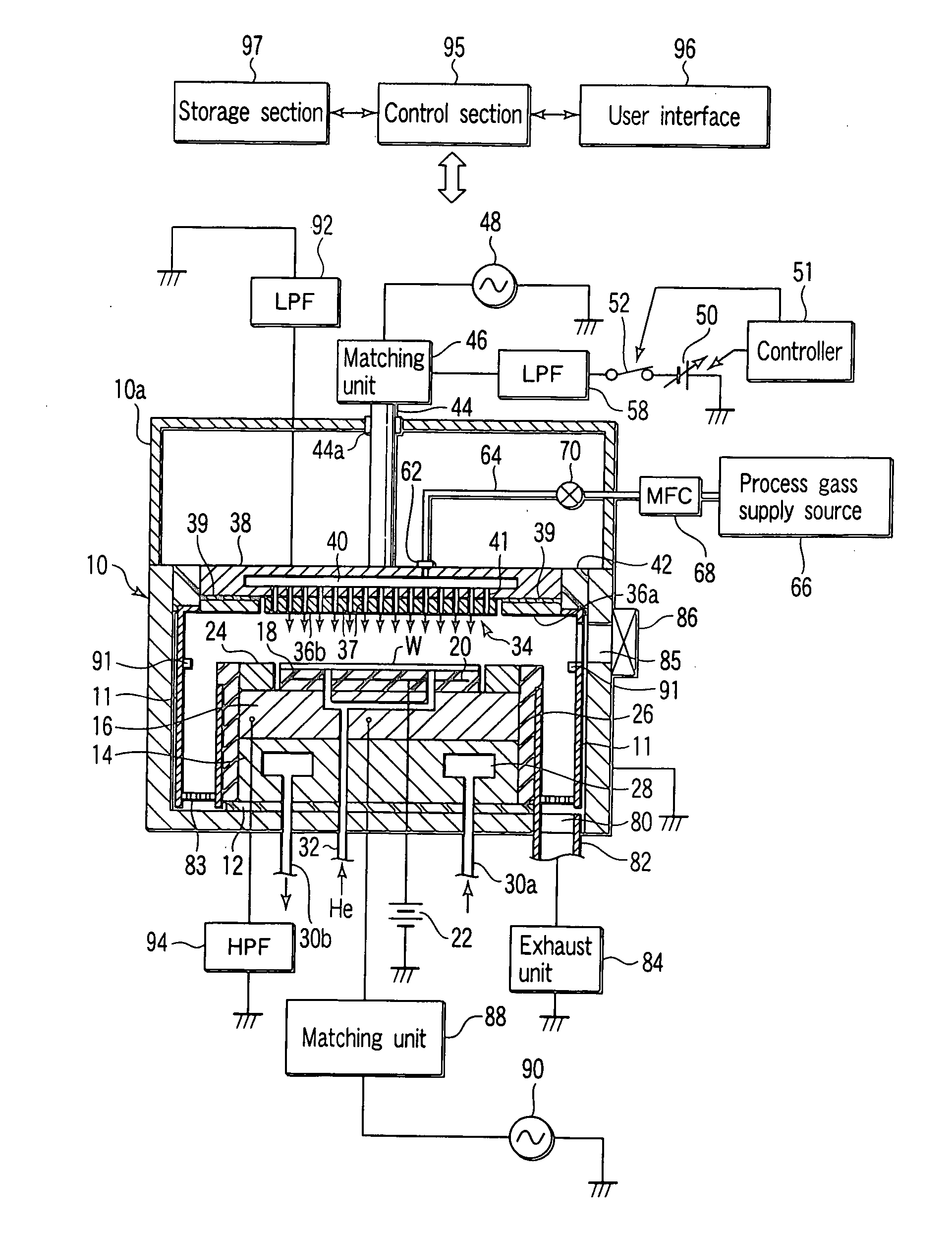
[0055]FIG. 1 is a sectional view schematically showing a plasma etching apparatus according to a first embodiment of the present invention. This plasma etching apparatus is structured as a parallel-plate plasma etching apparatus of the capacitive coupling type. The apparatus includes a cylindrical chamber (process container) 10, which is made of, e.g., aluminum with an anodization-processed surface. The chamber 10 is protectively grounded.

[0056] A columnar susceptor pedestal 14 is disposed on the bottom of the chamber 10 through an insulating plate 12 made of, e.g., a ceramic. A susceptor 16 made of, e.g., aluminum is disposed on the susceptor pedestal 14. The susceptor 16 is used as a lower electrode, on which a target substrate, such as a semiconductor wafer W, is placed.

[0057] The susceptor 16 is provided with an electrostatic chuck 18 on the top, for holding the target substrate or semiconductor wafer W by an electrostatic attraction force. The electrostatic chuck 18 comprises...

second embodiment

[0088]FIG. 4 is a sectional view schematically showing a plasma etching apparatus according to a second embodiment of the present invention. In place of the upper electrode 34 of the first embodiment, this embodiment includes an upper electrode 34′ having the following structure. Specifically, the upper electrode 34′ comprises an outer upper electrode 34a and an inner upper electrode 34b. The outer upper electrode 34a has a ring shape or doughnut shape and is disposed to face a susceptor 16 at a predetermined distance. The inner upper electrode 34b has a circular plate shape and is disposed radially inside the outer upper electrode 34a while being insulated therefrom. The outer upper electrode 34a is separated from the inner upper electrode 34b by an annular gap (slit) of, e.g., 0.25 to 2.0 mm, in which a dielectric body 72 made of, e.g., quartz is disposed. An insulating shield member 42 made of, e.g., alumina (Al2O3) and having a ring shape is airtightly interposed between the out...

third embodiment

[0100]FIG. 6 is a sectional view schematically showing a plasma etching apparatus according to a third embodiment of the present invention. This embodiment is the same as the second embodiment except that a lower feed rod 76 is provided with a variable capacitor 78 that can adjust its capacitance, and an outer upper electrode 34a includes no dielectric film between an outer electrode plate 136a and an electrode support 38a. The variable capacitor 78 can adjust the balance between the outer electric field intensity and inner electric field intensity, as described later.

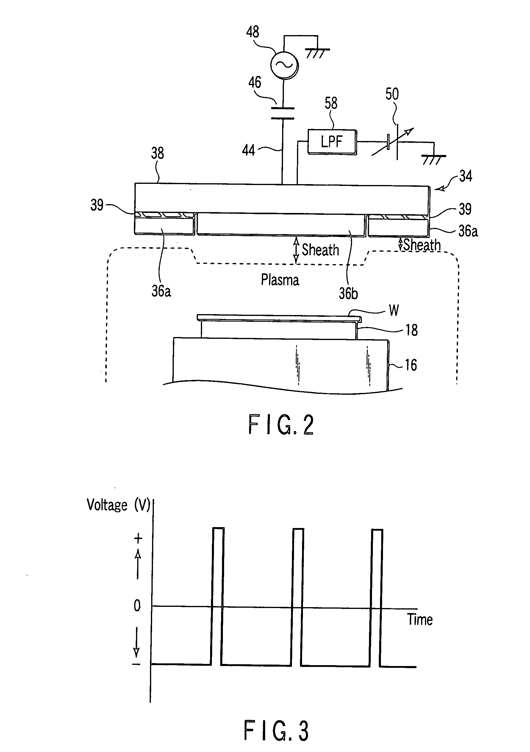
[0101]FIG. 7 is a diagram showing the upper electrode structure of the plasma etching apparatus shown in FIG. 6. In this embodiment, as schematically shown in FIG. 7, the upper electrode 34′ is formed of an outer upper electrode 34a and an inner upper electrode 34b separated from each other. A first RF power supply 48 is connected to the outer upper electrode 34a and inner upper electrode 34b through an upper feed rod...


PUM

PropertyMeasurementUnit
frequenciesaaaaaaaaaa
frequencyaaaaaaaaaa

Abstract

A plasma processing apparatus includes a process container configured to accommodate a target substrate and to be vacuum-exhausted. A first electrode and a second electrode are disposed opposite each other within the process container. The first electrode includes an outer portion and an inner portion both facing the second electrode such that the outer portion surrounds the inner portion. An RF power supply is configured to apply an RF power to the outer portion of the first electrode. A DC power supply is configured to apply a DC voltage to the inner portion of the first electrode. A process gas supply unit is configured to supply a process gas into the process container, wherein plasma of the process gas is generated between the first electrode and the second electrode.

Description

CROSS-REFERENCE TO RELATED APPLICATIONS [0001] This application claims the benefit of U.S. Provisional Application No. 60 / 666,710, filed Mar. 31, 2005. [0002] This application is based upon and claims the benefit of priority from prior Japanese Patent Application No. 2005-102953, filed Mar. 31, 2005, the entire contents of which are incorporated herein by reference.BACKGROUND OF THE INVENTION [0003] 1. Field of the Invention [0004] The present invention relates to a plasma processing apparatus of the capacitive coupling type and a method for using the same, used for performing a plasma process on a target substrate in, e.g., a semiconductor processing system. The term “semiconductor process” used herein includes various kinds of processes which are performed to manufacture a semiconductor device or a structure having wiring layers, electrodes, and the like to be connected to a semiconductor device, on a target substrate, such as a semiconductor wafer or a glass substrate used for an...

Claims


Application Information

Patent Timeline
Patent Type & Authority Applications(United States)
IPC IPC(8): C23F1/00C23C16/00
CPCC23F4/00H01L21/67069H01J37/32082H01J37/3244H01J37/32532H01J2237/334
Inventor MATSUMOTO, NAOKIKOSHIMIZU, CHISHIOKOSHIISHI, AKIRA
Owner TOKYO ELECTRON LTD
Why Eureka
Try Eureka