
Method for providing uniform distribution of plasma density in a plasma treatment apparatus

a plasma treatment and uniform distribution technology, applied in the field of semiconductor wafer production, can solve the problems of increasing the surface area of the wafer by 2.25 times, unable to meet the requirements of etching process plasma density, and extra high voltage, and achieve the effect of high plasma density

Active Publication Date: 2015-07-30
GLUKHOY YURI
View PDF2 Cites 36 Cited by
  • Summary
  • Abstract
  • Description
  • Claims
  • Application Information

AI Technical Summary

Benefits of technology

The present invention is about a method for creating a uniform distribution of plasma density in a plasma treatment of semiconductor wafers. This is particularly useful when treating large objects using plasma generated between a showerhead and the object. The invention improves the accuracy and effectiveness of plasma treatment, resulting in better quality semiconductor wafers.

Problems solved by technology

Therefore, the wafer surface area has increased by 2.25 times, and providing the required plasma density for the etching process becomes a problem.
This occurs because after exceeding some critical value, further increase of RF power will lead to extra high voltage and to electrical breakdown and arcing inside the plasma processing chamber.
This drastically reduces reliability and cost of the system.
However, at frequencies much higher than 13.56, the electromagnetic effects cause some problems that deteriorate the uniformity of plasma density.
All of these factors cause drastic changes in distribution of plasma density and ion flux and eventually result in nonuniformity of etching.
More specifically, exceeding the threshold gap depth leads to the same instability that occurs when frequency exceeds rated value.
Furthermore, the polished contact surfaces at the periphery cannot be ideally even and may be contaminated.
Therefore, in an actual application we should expect that some RF power can be lost and some gas may leak through the gaps.
The plasma that is used for etching semiconductor wafers is very corrosive.
Naturally, a showerhead that is used in such a process is subject to the effect of very chemically corrosive gasses, especially when etching the wafers with highly reactive radicals, and therefore the showerhead is subject to deterioration by chemical corrosion.
Moreover, heavy ions generated during plasma discharge bombard the sharp edges at the exits of the gas holes where electrical strength is very high.
As a result, such exits are converted into craters, and this violates the etching process.
However, the showerhead is a very expensive item.
As a result, the uniformity of plasma density further deteriorates, which results in poor planar uniformity and charge-up damage to the plasma etching.
With the increase of showerhead size and much higher frequency requested to support the optimal level of plasma density for maintaining uniformity in dual frequency, capacitively coupled plasma-etching systems become more complicated because of the electromagnetic and finite wavelength effects that deteriorate this uniformity.
As RF frequency increases, the plasma-effective wavelength decreases, and therefore the uniformity of the electrical field worsens.
Moreover, transition to sufficiently high frequencies shortens the wavelength and leads to some constructive and destructive interferences and skin effects.
Therefore, depending on the frequency, the finite wavelength produces nonuniformities that are already problematic for 300-mm showerheads, and will become more critical for showerheads used in apparatuses treating wafers of 450 mm.
This phenomenon causes interference of the aforementioned wave with the counter-propagating waves reflected from the rear sides of the showerhead.
Such changes in RF power distribution result in nonuniform RF power deposition into plasma.
As a result, the wafer treatment processes such as etching or deposition become nonuniform as well.
A drawback of this method is erosion and sputtering of the dielectric layer during the plasma process.
Another drawback is contamination of the wafer by the sputtered material.
However, the high resistivity part of the showerhead consumes too much RF power during Joule heating, and this reduces the efficiency of the device.
As a result, it becomes more difficult to adjust the uniformity of plasma density.
A drawback of this method is a complicated, real-time control of plasma uniformity that includes tuning the phases by oscillating the phases of the segments or the phase swapping to shift the pick of RF power distribution from the center to the middle.
The metal ceramic neighboring at the processing surface of the showerhead deteriorates the plasma sheath, and the resulting sputtering and erosion contaminate the product.
However, manufacture of the showerhead with an accurate and smooth curvilinear surface is an extremely complicated, inefficient, and expensive procedure.
It is understood in this regard that in transition to 450-mm wafer etching systems, the above methods and constructions are less efficient than methods based on controlling gas distribution.
However, changing the geometry at the exits of the holes on the processing side of the showerhead is not recommended (see, for example, U.S. Pat. No. 6,333,601 issued to S. Wickramanayaka on Dec. 25, 2001, “Planar gas introducing unit of a CCP reactor”).
These ions gain high energy, especially in vicinity of the sharp edges of the gas holes where density of the electrical field is high; thus, the bombardment of ions on the surface causes sputtering of this surface.
This process causes an erosion of the gas hole compared to the other areas of the showerhead, resulting in an enlargement in the diameter of the gas holes.
However, during wafer processing, such as plasma etching, the showerhead and cooler plate are heated, and the difference in their thermal expansions places high loads on the O-rings.
Besides a high temperature, the O-ring is also exposed to a highly corrosive etching gas.
As a result, the O-ring material degrades, thus contaminating the etching process.
Because processing gas leaks through the deteriorated O-ring, the pressure in each zone becomes out of control, and the etching process is deteriorated.
However, the apparatus has a complicated structure, strict tolerances, and must be very carefully designed just for a single-process protocol.
Another factor that causes nonuniformity of plasma treatment is deterioration of gas distribution channels that supply the processing gas from gas accumulation to plasma treatment through the showerhead.
However, since a showerhead surface is under high-voltage RF, the plasma treatment procedure is jeopardized by the highly destructive electrical processes.
More specifically, instabilities in the RF circuit that are caused by many reasons may lead to generation of very high frequency in RF power.
The gas in the reservoir is also susceptible to electrical breakdown.
This leads to the loss of power and distortion of the passage geometry, and, hence, to instability in technological parameters of the process.
This leads to drastic lowering of the resistance of silicon to sputtering and etching.
Such a mismatching may be caused by variations in chamber pressure, RF power, etc.
This arcing leads to destruction of the showerhead and, hence, to nonuniform distribution of processing gas in the plasma cavity, as well as to contamination of processing gas and of the product with particles of the showerhead material.
It should be further noted that the deterioration described above is not uniform and has a different degree in different areas of the showerhead.
This leads to shortening of the channel lengths in the peripheral part of the showerhead, which leads to decrease in gas pressure in the space in the peripheral areas of the processing chamber.
This, in turn, leads to the nonuniformity of plasma.

Method used


Image

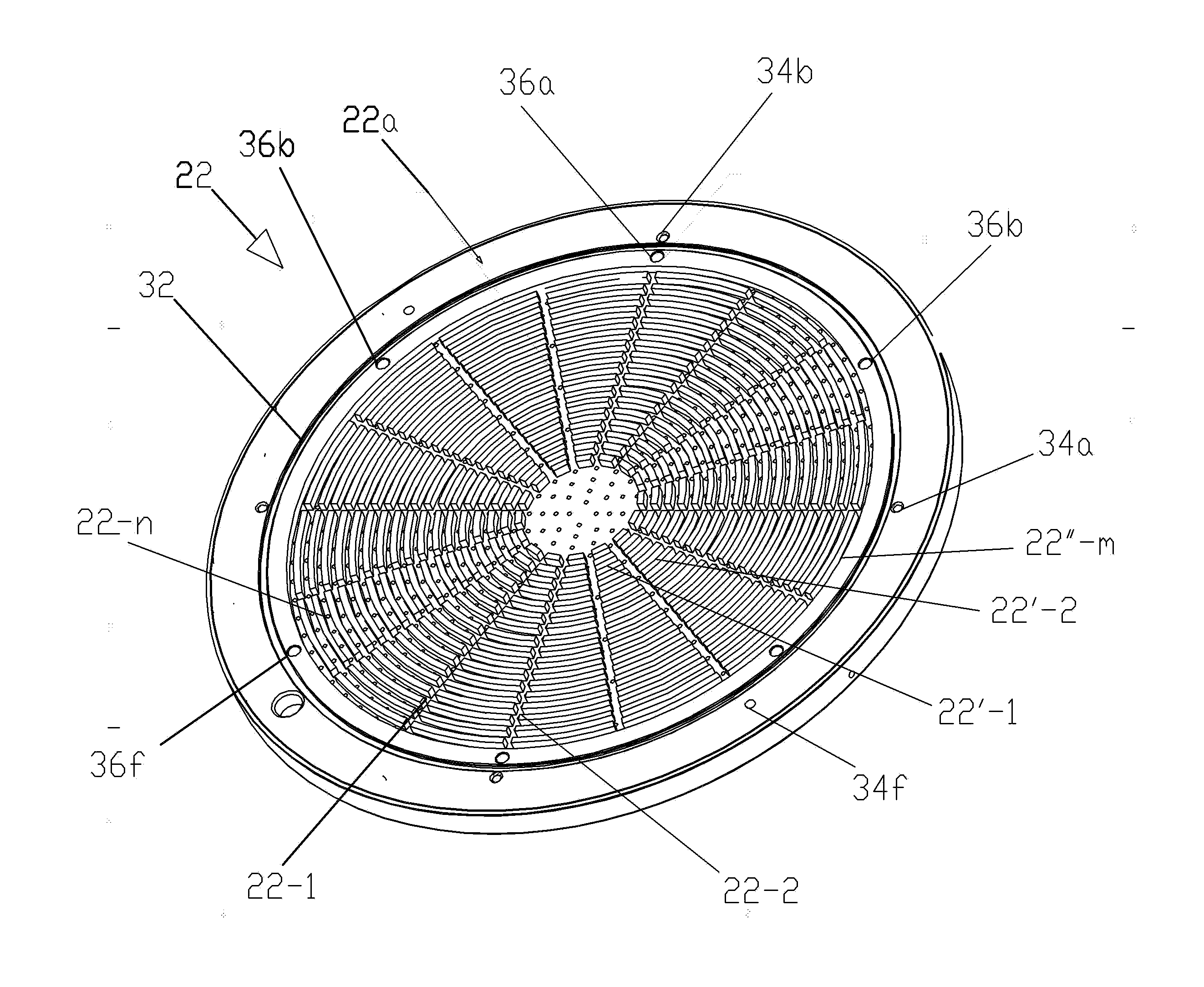
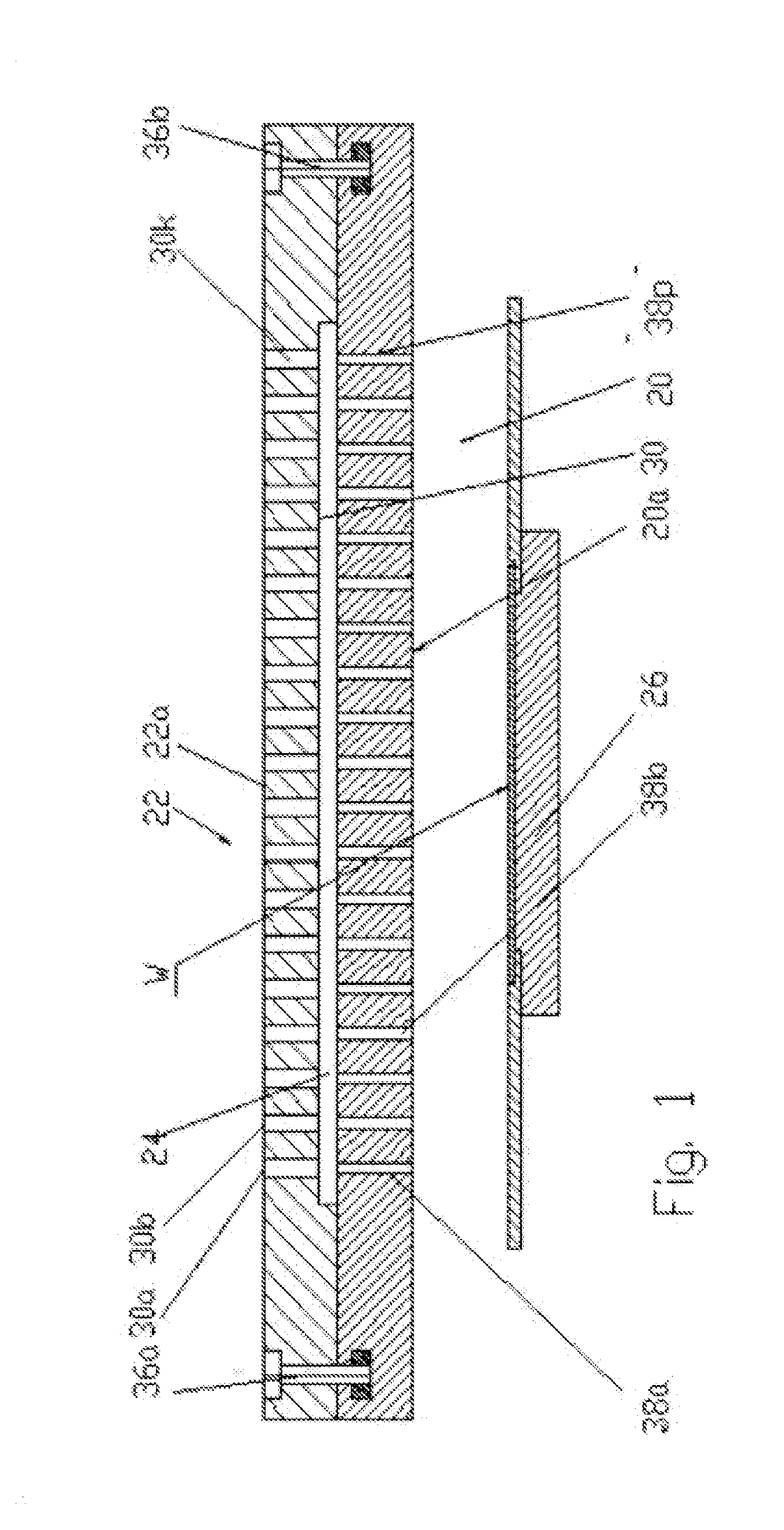
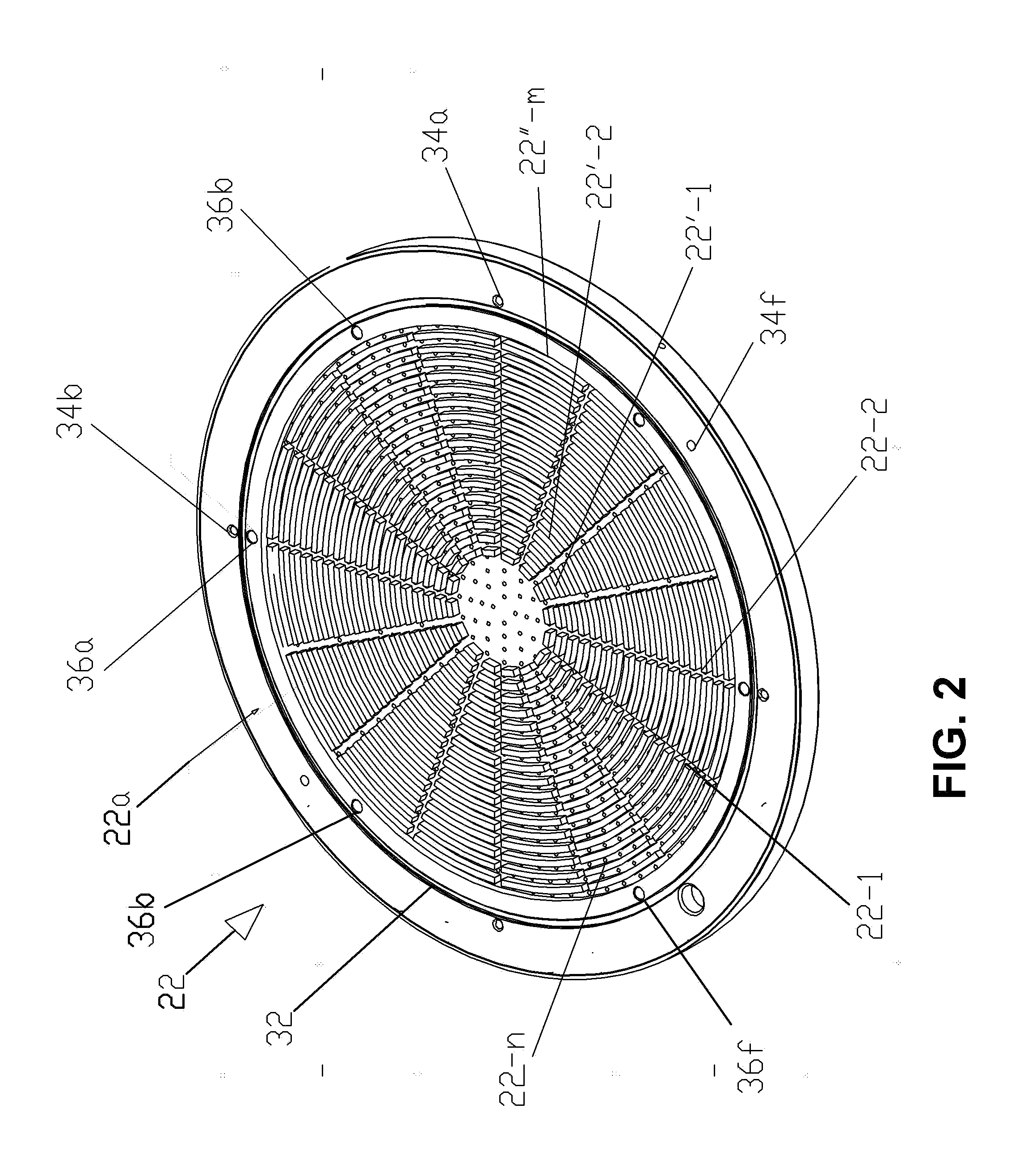
  • Method for providing uniform distribution of plasma density in a plasma treatment apparatus
  • Method for providing uniform distribution of plasma density in a plasma treatment apparatus
  • Method for providing uniform distribution of plasma density in a plasma treatment apparatus

Examples


Embodiment Construction

[0105]The invention relates to the field of semiconductor production, in particular to a method for providing uniform distribution of plasma density in a plasma treatment of semiconductor wafers in ICP plasma treatment apparatus. More specifically, the invention relates to a method for high uniformity of plasma generated in the plasma process chamber between the showerhead and an object being treated, especially in plasma process chambers for treating large area objects where the size of the showerhead becomes approximately on the same order as the wavelength of the plasma generating RF field.

[0106]The method of the invention comprises the steps of: providing a showerhead-cooler system of a semiconductor-processing chamber of the CCP plasma processing apparatus intended for plasma processing of objects, wherein the system comprises a showerhead having a plurality of through gas holes and a gas-feeding cooler plate that is connected to an RF power supply, has an electric contact with...


PUM

PropertyMeasurementUnit
diameteraaaaaaaaaa
diameteraaaaaaaaaa
frequencyaaaaaaaaaa

Abstract

Proposed is a method for providing uniform distribution of plasma density in a CCP plasma processing apparatus. According to the method the through gas holes of the showerhead of used in the plasma processing chamber of the apparatus are provided with conical nozzles formed on the side of the gas holes that face the gas reservoir of the cooler plate. The cone angle θ of the nozzles decreases in the direction from the peripheral portion to the central area of the showerhead in the range from 120° to 0°. Since the conical nozzles increase the gas gap between the showerhead and the cooler plate, more favorable conditions are created for electric breakdown. In order to protect the surfaces of the conical nozzles and gas holes from deterioration by hollow cathode discharge, these surface are coated by a protective coating resistant to electrical breakdown and chemical corrosion.

Description

FIELD OF THE INVENTION[0001]The invention relates to the field of semiconductor production, in particular to a method for providing uniform distribution of plasma density in a plasma treatment of semiconductor wafers in ICP plasma treatment apparatus. More specifically, the invention relates to a method for high uniformity of plasma generated in the plasma process chamber between the showerhead and an object being treated, especially in plasma process chambers for treating large area objects where the size of the showerhead becomes approximately on the same order as the wavelength of the plasma generating RF field.DESCRIPTION OF RELATED ART AND BACKGROUND OF THE INVENTION[0002]The fabrication of integrated circuits (IC) in the semiconductor industry typically employs plasma discharge, especially a capacitively coupled plasma (CCP) discharge, to create and assist surface chemistry within a processing chamber necessary to remove material from and deposit material onto a substrate. Waf...

Claims


Application Information

Patent Timeline
Patent Type & Authority Applications(United States)
IPC IPC(8): H01J37/32
CPCH01J37/32449H01J2237/04H01J2237/0213H01J37/32807B05D7/22C23C14/083C23C16/405H01J37/32091H01J37/32477Y10T29/4998
Inventor GLUKHOY, YURI
Owner GLUKHOY YURI
Learn More