Phase locked loop circuits, offset PLL transmitters, radio frequency integrated circuits and mobile phone systems

a phase lock loop and characteristics detection technology, applied in the direction of angle modulation, pulse automatic control, electrical apparatus, etc., can solve the problems of large scale of the circuit, reducing analog accuracy, and inability to perform fine frequency configuration, etc., to achieve optimal loop band-width, short time period, and high precision

Inactive Publication Date: 2006-10-05
RENESAS ELECTRONICS CORP
View PDF4 Cites 13 Cited by
  • Summary
  • Abstract
  • Description
  • Claims
  • Application Information

AI Technical Summary

Benefits of technology

[0031] According to the present invention, since the charge pump current can be changed through the result of the measurement of the loop gain of the PLL circuit, a calibration system can be provided which can configure an optimal loop band-width in a short amount of time and with high precision. In addition, the present invention has the advantage that it is applicable not only to the fractional-N PLL but also to various types of PLLs.

Problems solved by technology

Thus, it is required that the oscillating frequency of the VCO be set up at 200 kHz intervals; however, since the division ratio is an integer, the frequency of the VCO can only take the value, which is an integer multiple of the reference frequency, so that a fine frequency configuration cannot be performed.
Conventionally, external parts were used for the loop filter circuit employed for the PLL circuit because, in addition to the number of elements such as resistance and capacitance being large, when integrated in the LSIs, the analog accuracy is lowered due to the variation of elements that cause deterioration of the calibration accuracy, the scale of the circuit becomes large, and it takes time to calibrate.
However, downsizing is always required for mobile communication equipment.
The reduction of external parts is one of the serious problems in promoting the integration and downsizing of mobile communication equipment.

Method used


Image

  • Phase locked loop circuits, offset PLL transmitters, radio frequency integrated circuits and mobile phone systems
  • Phase locked loop circuits, offset PLL transmitters, radio frequency integrated circuits and mobile phone systems
  • Phase locked loop circuits, offset PLL transmitters, radio frequency integrated circuits and mobile phone systems

Examples


first embodiment

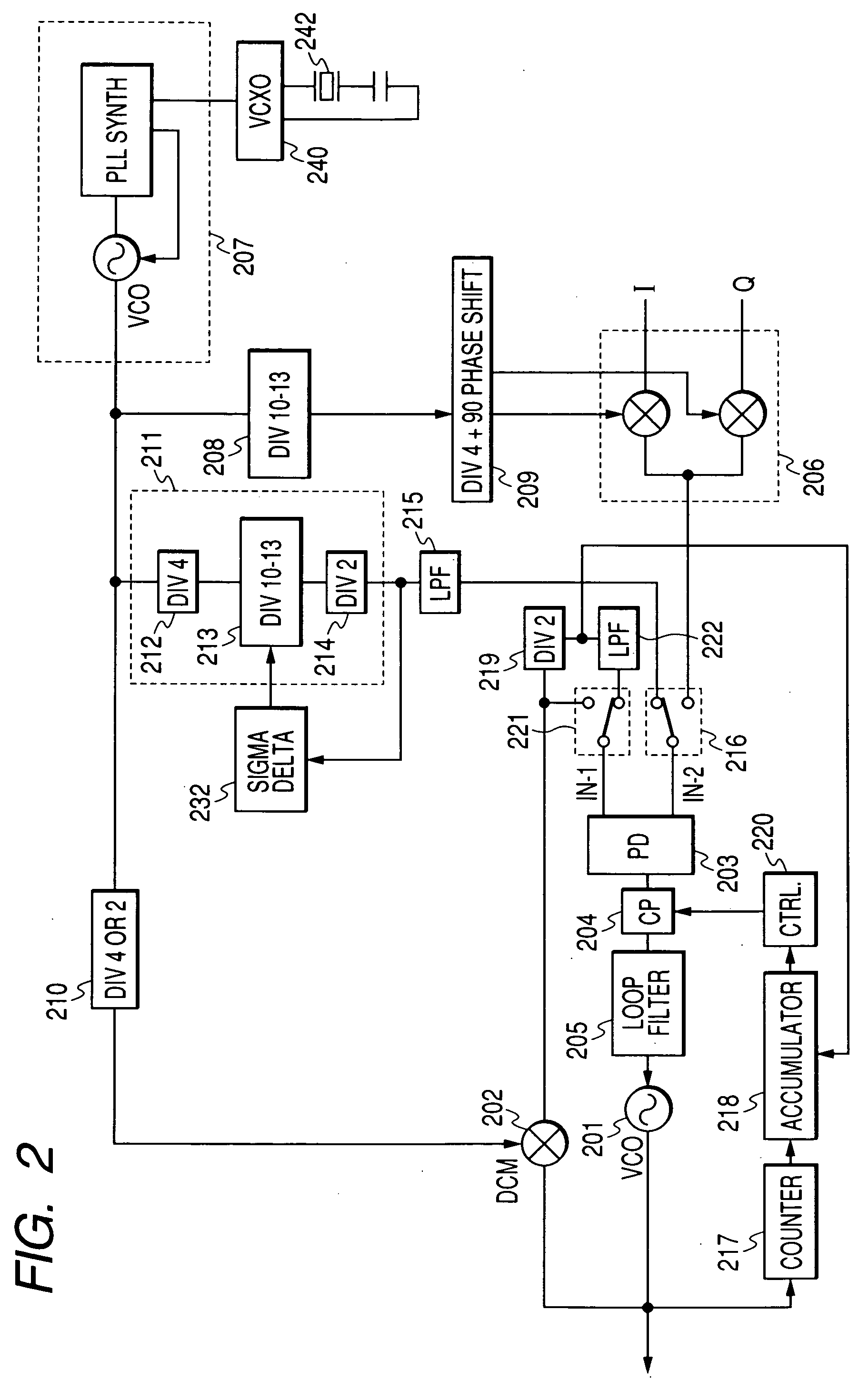
[0071] The first embodiment according to the present invention will be illustrated by using FIGS. 2 to 7. The present embodiment is such that a step waveform is input into the offset PLL-type phase locked loop circuit to detect the response by the output of voltage locked oscillator 201.

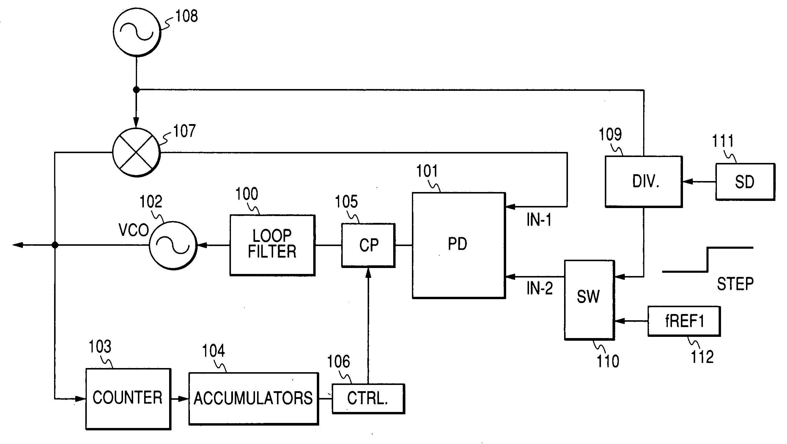
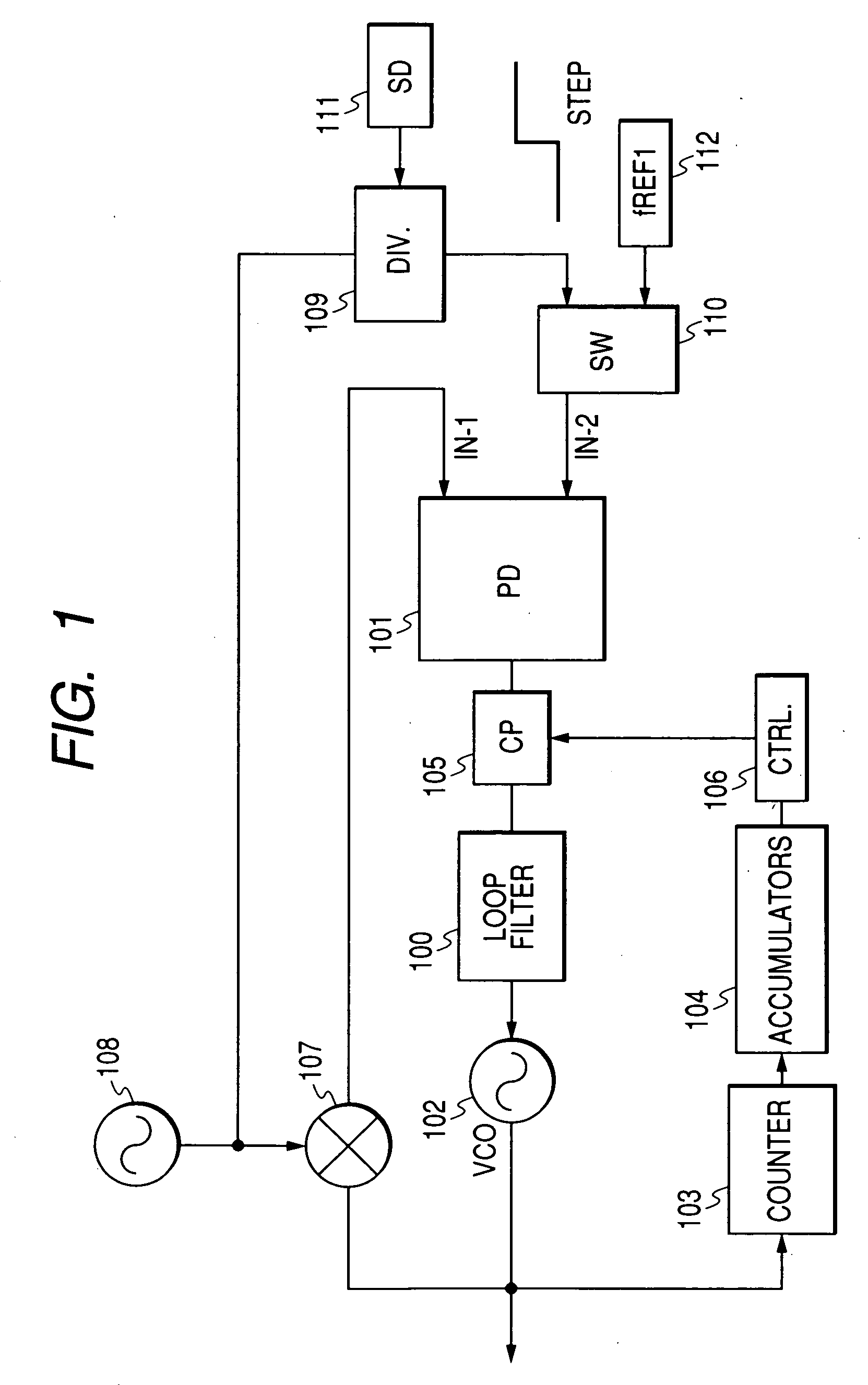
[0072] Firstly, in FIG. 2, the entire configuration and operation of the offset PLL-type phase locked loop circuit and the offset PLL transmitter, including the above, will be illustrated. Firstly, the configuration of the offset PLL and its theory of operation will be briefly described. The offset PLL-type phase locked loop circuit is composed of voltage locked oscillator (VOC) 201, down conversion mixer (DCM) 202, phase detector (PD) 203, charge pump (CP) 204, and loop filter (LF) 205.

[0073] In the first input (IN-1) of phase detector 203 of the PLL circuit, the output of VCO 201, is input through switch 221. The output of VCO 201 is compared with the first reference signal (fREF1), which was inp...

first modification

[0105] In FIG. 3, the explanations are given on the assumption that the integration time by integrator 218 in the phase locked loop circuit of FIG. 1, that is, time T1 from the integration value zero to terminal B in waveform 307 is equal to time T2 from the integration value zero to terminal A in waveform 306. However, as a modified example of the first embodiment, it is possible to improve the proportional relation between the difference value (B-A) and the reciprocal (1 / Loop-gain) of the loop gain by optimizing the relation between integration times T1 and T2.

second modification

[0106] Integrator 218 in the phase locked loop circuit in the first embodiment is composed of a single stage; however, it is allowable to configure it so that multistage integrators be connected instead and the difference value (B-A) obtained in the preceding integrator is synchronized by the subsequent integrator to further perform integration. Through these configurations, the characteristics of the proportional relation between the difference value (B-A) and the reciprocal (1 / Loop-gain) of the loop gain is further improved to enhance the accuracy of detecting loop characteristics.

[0107] In addition, as for the means to compensate for the delay caused in the process of generating the first reference signal, in the first embodiment, sigma delta modulator 232 generates the step signal whose division number of divider 211 is changed in the phase locked loop circuit; however, the configuration is not limited thereto.


PUM


Abstract

A PLL circuit equipped with a loop gain detecting circuit that can suppress the change of the loop gain. When detecting the loop gain, the frequency of the input signal to the second input (IN-2) of the phase detector is first changed, and the response corresponding to the change is detected by the output of the voltage locked oscillator. The detection is performed by connecting the output of the voltage locked oscillator with the counter and connecting the output of the counter with the integrator. The phase locked loop characteristics are optimized by performing feedback for the detection result on the value of the charge pump current.

Description

CLAIM OF PRIORITY [0001] The present application claims priority from Japanese application JP 2005-094161 filed on Mar. 29, 2005 and Japanese application JP 2005-326340 filed on Nov. 10, 2005, the contents of which are hereby incorporated by reference into this application. CROSS-REFERENCE TO RELATED APPLICATION [0002] This application is related to U.S. application Ser. No. 11 / 202266, filed on Aug. 12, 2005, the disclosure of which is hereby incorporated by reference. FIELD OF THE INVENTION [0003] The present invention relates to a loop characteristics detecting circuit of a phase locked loop (PLL) circuit, more particularly to an offset PLL transmitter, radio frequency integrated circuit, and mobile phone system having a PLL circuit which is equipped with a loop gain detecting circuit based on the loop gain detecting method of a phase locked loop circuit and its detecting method. BACKGROUND OF THE INVENTION [0004] A transmitter circuit employing a PLL is described, for example, in...

Claims


Application Information

Patent Timeline
Patent Type & Authority Applications(United States)
IPC IPC(8): H03L7/00
CPCH03C3/0933H03C3/0966H03C3/0983H03L7/185H03L7/0895H03L7/0898H03L7/107H03C3/0991H03L7/1072
Inventor AKAMINE, YUKINORIKAWABE, MANABUTANAKA, SATOSHISHIMA, YASUOTAKANO, RYOICHI
Owner RENESAS ELECTRONICS CORP
Why Eureka
Try Eureka