Lithographic apparatus and device manufacturing method

a technology of lithographic apparatus and manufacturing method, which is applied in the direction of photomechanical apparatus, optical devices, instruments, etc., can solve the problems of inability to achieve absolute accuracy and in particular thermal stability over long travel ranges, reduce the throughput of lithographic apparatus, and take a considerable amount of time to achieve the effect of high accuracy

Active Publication Date: 2006-10-12
ASML NETHERLANDS BV
View PDF14 Cites 529 Cited by
  • Summary
  • Abstract
  • Description
  • Claims
  • Application Information

AI Technical Summary

Benefits of technology

[0013] It is desirable to provide a high accuracy displacement measuring system for a lithographic apparatus which is configured to measure the position of the substrate table in all possible locations making continuous measurement of the position of the substrate table possible.

Problems solved by technology

One of the most challenging requirements for micro-lithography for the production of integrated circuits as well as liquid crystal display panels is the positioning of tables.
Although such sensors can provide sub-micrometer level resolution without difficulty, absolute accuracy and in particular thermal stability over long travel ranges are not readily achievable.
This takes a considerable amount of time, and as a result the throughput of the lithographic apparatus is decreased.
However, the sensor range of such sensor is in principle limited to the size of the grid plate.
However, the size of such grid plate is physically limited due to the high resolution required in the grid.
Thus, in practice the size of the working area of such sensor is limited.
At the location of such hole / opening, a sensor cannot determine its position.
Moreover, it is possible that the grid plate is locally damaged, which may make an accurate determination of the position of a sensor on this position impossible.

Method used


Image

  • Lithographic apparatus and device manufacturing method
  • Lithographic apparatus and device manufacturing method
  • Lithographic apparatus and device manufacturing method

Examples


Embodiment Construction

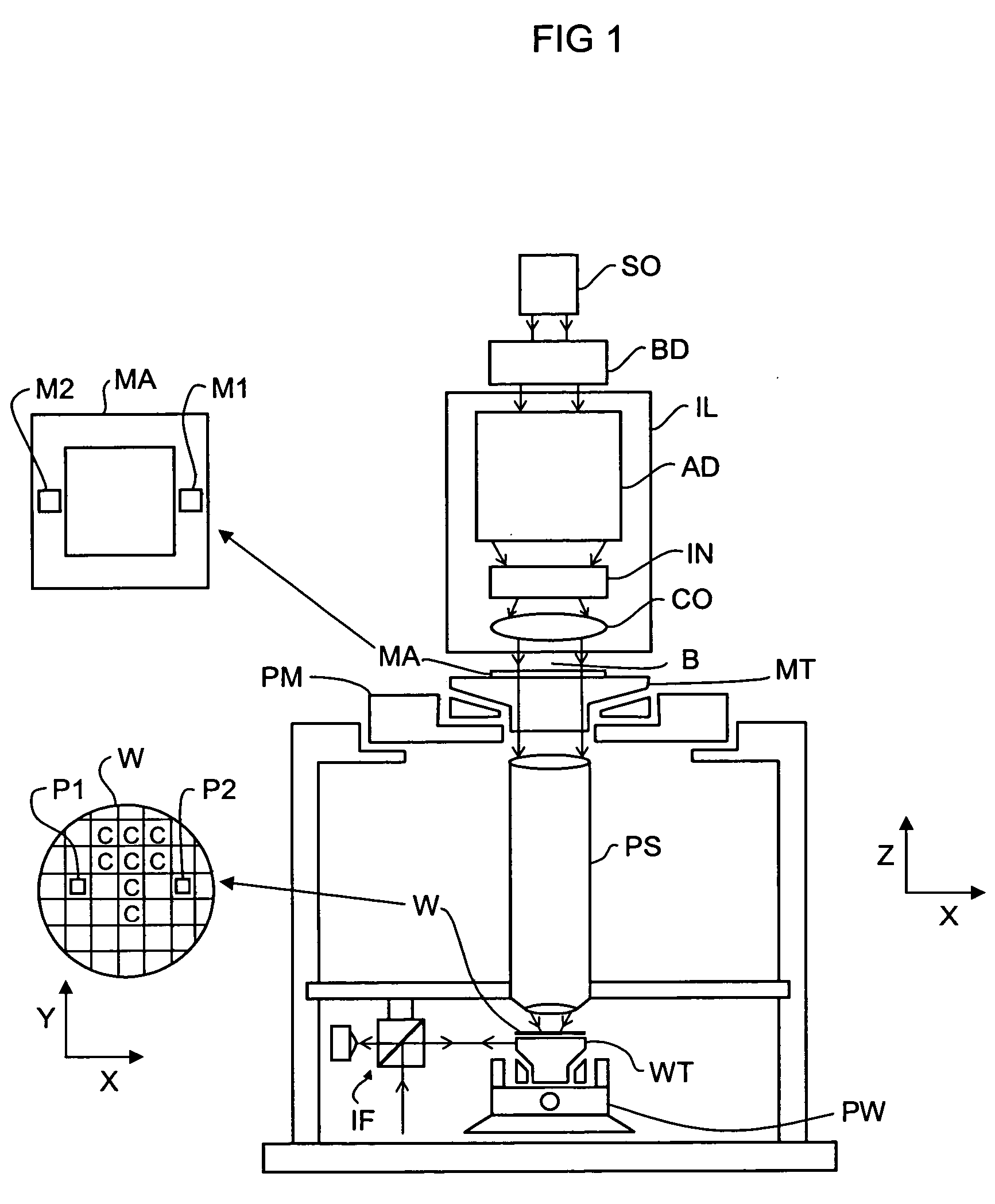
[0031]FIG. 1 schematically depicts a lithographic apparatus according to one embodiment of the invention. The apparatus includes an illumination system (illuminator) IL configured to condition a radiation beam B (e.g. UV radiation or any other suitable radiation), a mask support structure (e.g. a mask table) MT constructed to support a patterning device (e.g. a mask) MA and connected to a first positioning device PM configured to accurately position the patterning device in accordance with certain parameters. The apparatus also includes a substrate table (e.g. a wafer table) WT or “substrate support” constructed to hold a substrate (e.g. a resist-coated wafer) W and connected to a second positioning device PW configured to accurately position the substrate in accordance with certain parameters. The apparatus further includes a projection system (e.g. a refractive projection lens system) PS configured to project a pattern imparted to the radiation beam B by patterning device MA onto ...


PUM


Abstract

A lithographic apparatus includes a displacement measuring system configured to measure the position of a substrate table in at least three degrees of freedom. The displacement measuring system includes a first x-sensor configured to measure the position of the substrate table in a first direction and a first and a second y-sensor configured to measure the position of the substrate table in a second direction. Said displacement measuring system further comprises a second x-sensor. The first and second x-sensor and first and second y-sensors are encoder type sensors configured to measure the position of each of the sensors with respect to at least one grid plate. The displacement measuring system is configured to selectively use, depending on the position of the substrate table, three of the first and second x-sensors and the first and second y-sensors to determine the position of the substrate table in three degrees of freedom.

Description

[0001] This application is a continuation in part of U.S. patent application Ser. No. 11 / 101,631, entitled “Dual Stage Lithographic Apparatus And Device Manufacturing Method”, filed on Apr. 8, 2005. The content of that application is incorporated herein in its entirety by reference.BACKGROUND [0002] 1. Field of the Invention [0003] The present invention relates to a lithographic apparatus and a method for manufacturing a device. [0004] 2. Description of the Related Art [0005] A lithographic apparatus is a machine that applies a desired pattern onto a substrate, usually onto a target portion of the substrate. A lithographic apparatus can be used, for example, in the manufacture of integrated circuits (ICs). In such a case, a patterning device, which is alternatively referred to as a mask or a reticle, may be used to generate a circuit pattern to be formed on an individual layer of the IC. This pattern can be transferred onto a target portion (e.g. including part of, one, or several d...

Claims


Application Information

Patent Timeline
Patent Type & Authority Applications(United States)
IPC IPC(8): G03B27/42
CPCG03F7/70775
Inventor LOOPSTRA, ERIK ROELOFVAN DER PASCH, ENGELBERTUS ANTONIUS FRANSISCUS
Owner ASML NETHERLANDS BV
Why Eureka
Try Eureka