Dual-hybrid liner formation without exposing silicide layer to photoresist stripping chemicals

a dual-hybrid, stripping technology, applied in the direction of basic electric elements, semiconductor devices, electrical equipment, etc., can solve the problems of reducing pfet performance, degrading electron mobility, and reducing hole mobility, so as to prevent the exposure of a suicide layer and good lateral dimension control

Inactive Publication Date: 2006-10-12
IBM CORP +1
View PDF10 Cites 35 Cited by
  • Summary
  • Abstract
  • Description
  • Claims
  • Application Information

AI Technical Summary

Benefits of technology

[0008] The invention includes methods of fabricating a semiconductor device including a dual-hybrid liner in which an underlying silicide layer is protected from photoresist stripping chemicals by using a hard mask as a pattern during etching, rather than using a photoresist. The hard mask prevents exposure of a suicide layer to photoresist stripping chemicals and provides very good lateral dimension control such that the two nitride liners are well aligned.

Problems solved by technology

However, tensile stress may degrade hole mobility and hence reduce PFET performance.
Similarly, compressive stress may degrade electron mobility and hence worsen NFET performance.
Unfortunately, photoresist stripping chemicals typically include oxygen or ozone that can cause oxidation of silicide layer 12 and increased resistance.
In technologies beyond 90 nm, which utilize ultra small gatelengths (e.g., s is unacceptable because it will impact performance of the device.

Method used


Image

  • Dual-hybrid liner formation without exposing silicide layer to photoresist stripping chemicals
  • Dual-hybrid liner formation without exposing silicide layer to photoresist stripping chemicals
  • Dual-hybrid liner formation without exposing silicide layer to photoresist stripping chemicals

Examples


Embodiment Construction

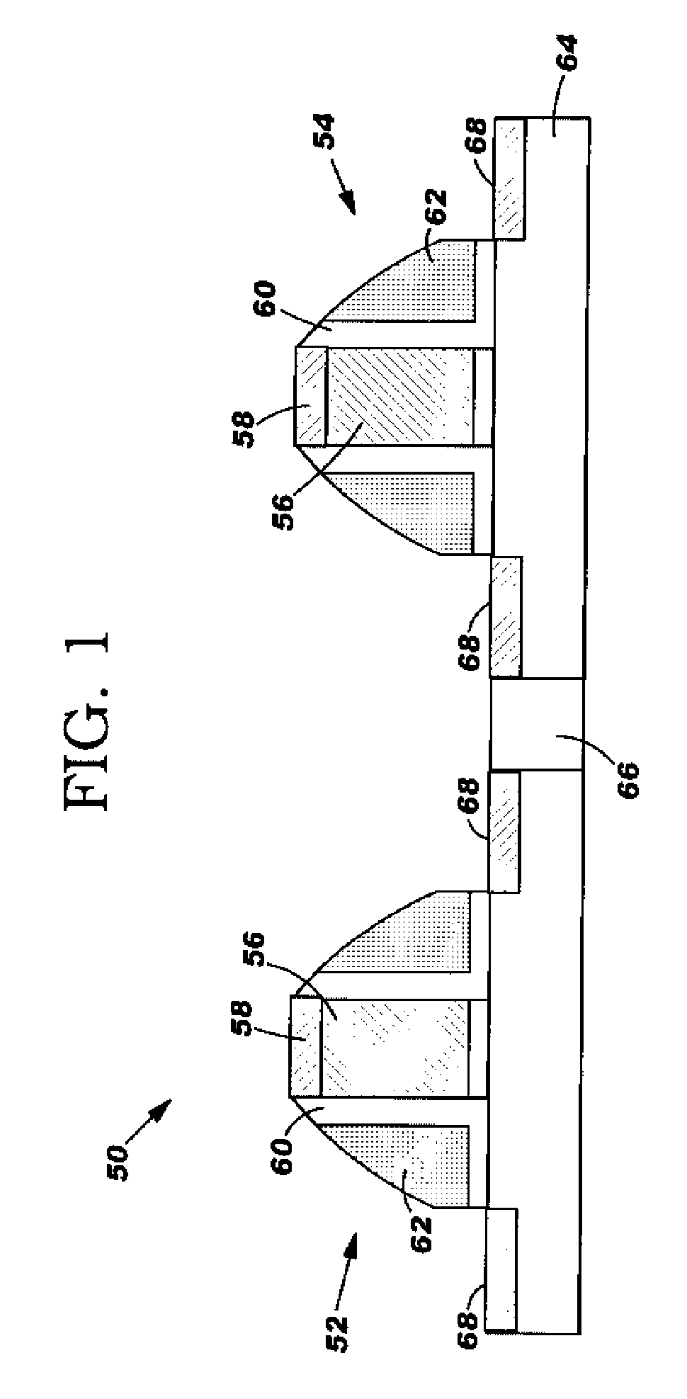
[0015] With reference to the accompanying drawings, FIG. 1 shows an initial structure 50 for a method of fabricating a semiconductor device including a dual-hybrid liner. Initial structure 50 includes a p-type field effect transistor (PFET) 52 and an n-type field effect transistor (NFET) 54. PFET 52 and NFET 54 each include a gate body 56 having a silicide cap 58, a silicon dioxide (SiO2) spacer 60 and a silicon nitride (Si3N4) spacer 62 formed over a substrate 64. A shallow trench isolation (STI) 66 separates the FETs 52, 54. An underlying silicide layer 68 is provided in an upper region of substrate 64. It should be recognized that the teachings of the invention are not limited to this initial structure. For example, while substrate 64 is illustrated as bulk silicon, it could also be provided in a silicon-on-insulator (SOI) form.

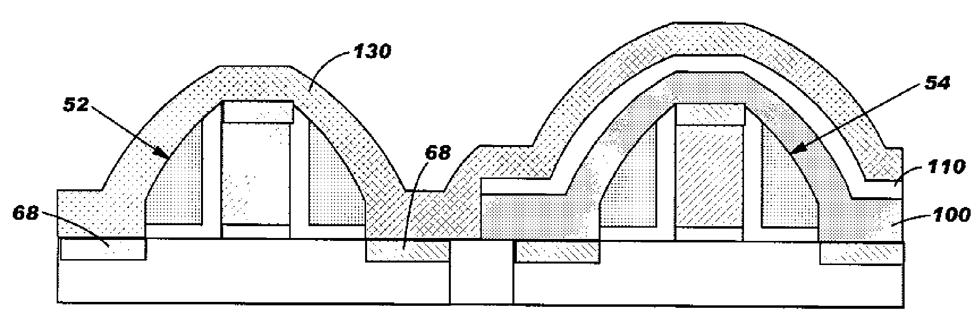
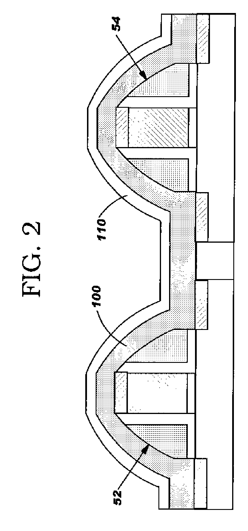
[0016] Turning to FIG. 2, a first step of the method includes depositing a first silicon nitride layer 100 (hereinafter “first SiN layer”) over PFET 52 a...


PUM


Abstract

Methods of fabricating a semiconductor device including a dual-hybrid liner in which an underlying silicide layer is protected from photoresist stripping chemicals by using a hard mask as a pattern during etching, rather than using a photoresist. The hard mask prevents exposure of a silicide layer to photoresist stripping chemicals and provides very good lateral dimension control such that the two nitride liners are well aligned.

Description

BACKGROUND OF THE INVENTION [0001] 1. Technical Field [0002] The present invention relates generally to semiconductor fabrication, and more particularly, to forming a dual-hybrid liner without exposing an underlying silicide layer to photoresist stripping chemicals. [0003] 2. Related Art [0004] The application of stresses to field effect transistors (FETs) is known to influence their performance. When applied in a longitudinal direction (i.e., in the direction of current flow), tensile stress is known to enhance electron mobility (or n-channel FET (NFET) drive currents) while compressive stress is known to enhance hole mobility (or p-channel FET (PFET) drive currents). One way to apply such stresses to a FET is the use of intrinsically-stressed barrier silicon nitride liners. For example, a tensile-stressed silicon nitride liner may be used to cause tension in an NFET channel while a compressively-stressed silicon nitride liner may be used to cause compression in a PFET channel. How...

Claims


Application Information

Patent Timeline
Patent Type & Authority Applications(United States)
IPC IPC(8): H01L21/471
CPCH01L21/76828H01L21/76829H01L21/76832H01L29/7843H01L29/66575H01L29/78H01L29/665
Inventor CHAN, VICTORYANG, HAINING S.LEE, YONG M.LIM, ENG H.
Owner IBM CORP
Why Eureka
Try Eureka