Holder manufacturing method for loading substrate of semiconductor manufacturing device, batch type boat having holder, loading/unloading method of semiconductor substrate using the same, and semiconductor manufacturing device having the same

a manufacturing method and semiconductor technology, applied in the direction of loading/unloading, basic electric elements, thin material processing, etc., can solve the problems of deteriorating semiconductor manufacturing device productivity, difficulty in molding process for ensuring the height of the supporting ring, inconvenience in manufacturing, etc., to achieve simple manufacturing, improve the effect of substrate treatment amount and productivity

Active Publication Date: 2006-10-26
WONIK IPS CO LTD
View PDF10 Cites 8 Cited by
  • Summary
  • Abstract
  • Description
  • Claims
  • Application Information

AI Technical Summary

Benefits of technology

[0035] Anther object of the present invention is to provide a batch type boat having the holder, in that the manufacture thereof is simple by means of a holder ring and the holder ring is supported on supporting rods and an end-effector escap

Problems solved by technology

However, the conventional holder 7 brings about the manufacturing inconvenience on account of the manufacturing difficulty of the holder itself.
However, there are various problems owing to the complexity of the peripheral device and so on.
However, since the manufacturing methods of the conventional holder uses the silicon carbide of a high-price, there is a problem in that the productivity of semiconductor manufacturing device is deteriorated.
However, in case of using the silicon carbide so as to co

Method used


Image

  • Holder manufacturing method for loading substrate of semiconductor manufacturing device, batch type boat having holder, loading/unloading method of semiconductor substrate using the same, and semiconductor manufacturing device having the same
  • Holder manufacturing method for loading substrate of semiconductor manufacturing device, batch type boat having holder, loading/unloading method of semiconductor substrate using the same, and semiconductor manufacturing device having the same
  • Holder manufacturing method for loading substrate of semiconductor manufacturing device, batch type boat having holder, loading/unloading method of semiconductor substrate using the same, and semiconductor manufacturing device having the same

Examples


Embodiment Construction

[0050] A preferred embodiment of the invention will be described in detail below with reference to the accompanying drawings.

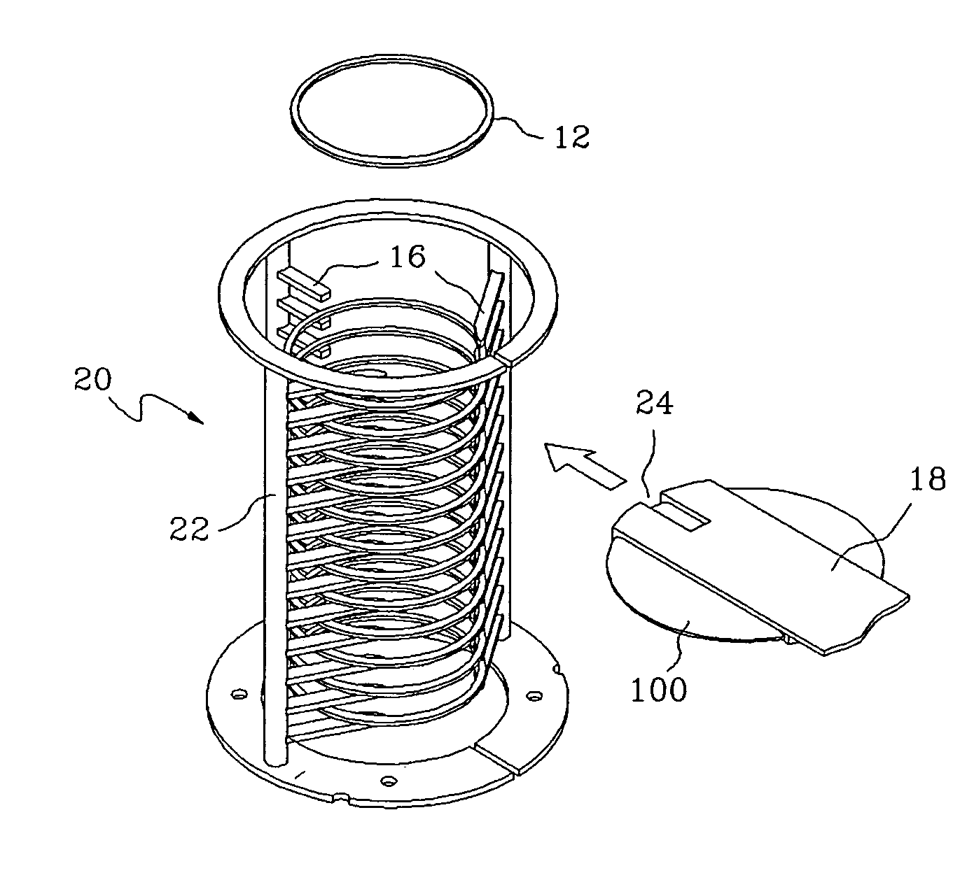
[0051]FIG. 4 is a conceptual view illustrating a manufacturing method of a holder ring according to the present invention. FIG. 5 is an explanatory view illustrating the external appearance of a semiconductor manufacturing device including a batch type boat having the holder rings and an end-effector of a top-edge-grip type according to one embodiment of the present invention. FIG. 6 is plan and side views of FIG. 5.

[0052] Also, FIG. 7 is an explanatory view illustrating the external appearance of a semiconductor manufacturing device including a batch type boat having the holder rings and an end-effector of a bottom-lift type according to another embodiment of the present invention. FIG. 8 is plan and side views of FIG. 7.

[0053] Firstly, as shown in FIG. 4, a holder according to the present invention includes a supporting panel of a circular plate type and ...


PUM


Abstract

A holder manufacturing method for loading a substrate of a semiconductor manufacturing device, a batch type boat having the holder, a loading/unloading method of a semiconductor substrate using the same, and a semiconductor manufacturing device having the same are disclosed. For example, the manufacturing method of the holder of the boat for loading a semiconductor substrate includes the steps of molding a holder substrate of a pipe shape having inner and outer circumference of a predetermined size in such a manner that a lower portion of the semiconductor substrate is seated thereon; and forming a plurality of holder rings by cutting the holder rings from the holder substrate in such a manner that each holder ring is matched to a disposal interval of the semiconductor substrates in the boat. The manufacture of the holder and the batch type boat are simple by means of the holder ring supported on the supporting rods and the end-effector escapes the supporting rods, so that the pitch interval can be minimized, whereby it can load the compact semiconductor substrate to the boat, the amount of the substrate treatment can be improved and thus the productivity thereof can be improved.

Description

BACKGROUND OF THE INVENTION [0001] 1. Field of the Invention [0002] The present invention relates to a holder manufacturing method for loading a substrate of a semiconductor manufacturing device, a batch type boat having the holder, a loading / unloading method of a semiconductor substrate using the same, and a semiconductor manufacturing device having the same. [0003] 2. Description of the Prior Art [0004] Generally, a semiconductor manufacturing device for treating the semiconductor substrate divides into a batch type including a boat for loading substrates in bulk therein in order to improve the processing capacity and a single wafer type for treating the process one by one in order to extremely decrease the processing time. [0005] In these processes, since the process time is consumed in order to increase or decrease the processing temperature, a semiconductor manufacturing device of the batch type is generally used in the manufacturing process thereof, especially a process of hig...

Claims


Application Information

Patent Timeline
IPC IPC(8): B65G25/00
CPCH01L21/67778H01L21/67306Y10S414/138
Inventor JANG, TAEK YOUNGLEE, BYOUNG IL
Owner WONIK IPS CO LTD
Why Eureka
Try Eureka