Test buffer design and interface mechanism for differential receiver AC/DC boundary scan test

a test buffer and ac/dc technology, applied in the field of boundary scan testing, can solve the problems of 1149.1 not addressing all situations, design practices, and conventional 1149.1 testing becoming impractical on ac coupled interconnections

Inactive Publication Date: 2006-10-26
CISCO TECH INC
View PDF7 Cites 6 Cited by
  • Summary
  • Abstract
  • Description
  • Claims
  • Application Information

AI Technical Summary

Problems solved by technology

However, 1149.1 does not address all situations and design practices.
The result is that conventional 1149.1 testing becomes impractical on AC coupled interconnections.

Method used


Image

  • Test buffer design and interface mechanism for differential receiver AC/DC boundary scan test
  • Test buffer design and interface mechanism for differential receiver AC/DC boundary scan test
  • Test buffer design and interface mechanism for differential receiver AC/DC boundary scan test

Examples


first embodiment

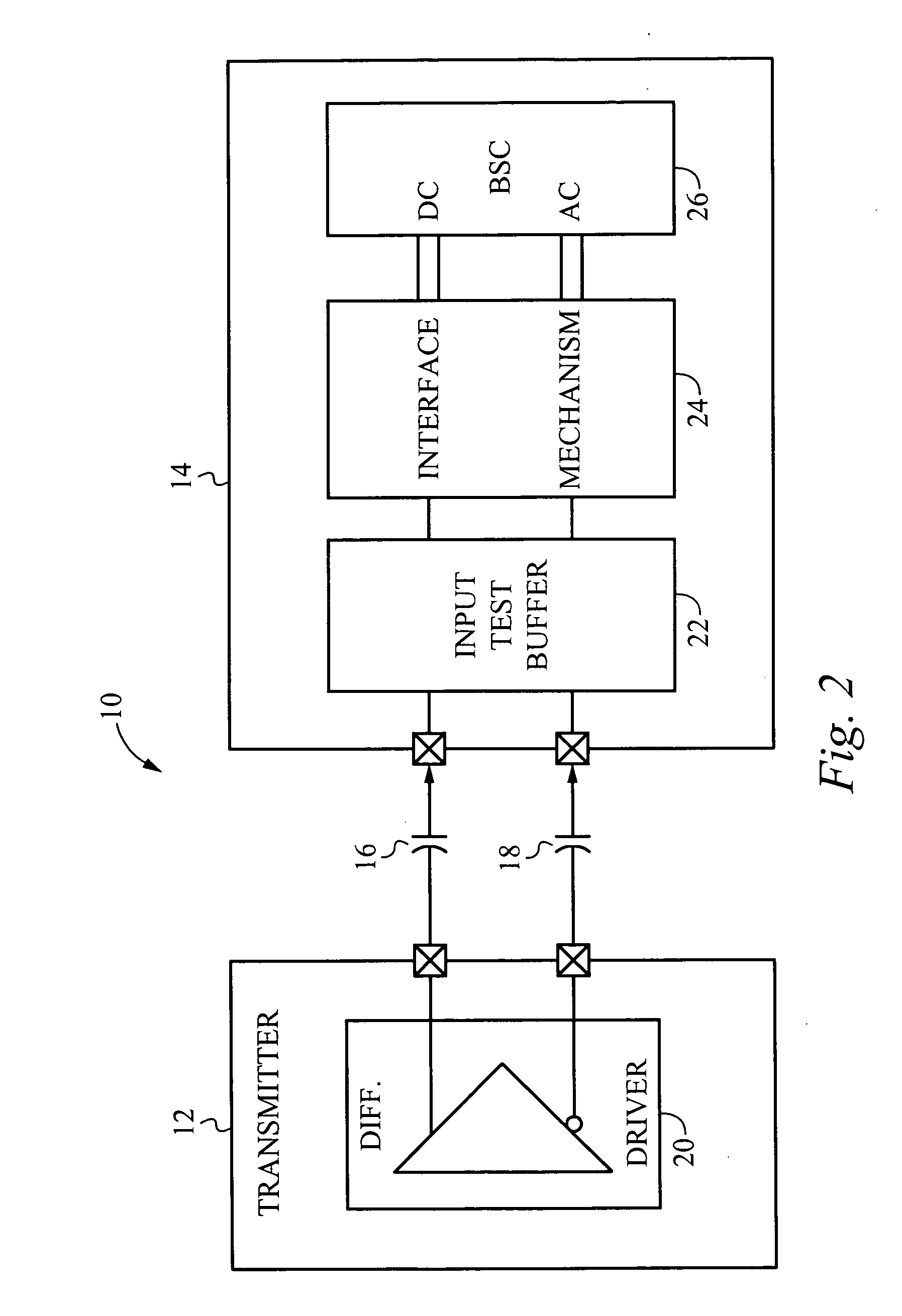
[0036] Turning now to FIG. 4, a block diagram of the input test buffer 22 of FIG. 2 is shown. The actual design of the input test buffer 22 can be selected from a number of designs available in the prior art. The one stipulation is that the design have built-in null detection capability, that is, if the differential voltage between the two signal inputs is not greater than a predefined threshold, then both of the output signals become the same value to identify a null condition. The null condition indicates that one of the five fault syndromes of FIG. 3 has been detected. Here the output signals have been labeled RESET and SET. The input test buffer 22 includes a first amplifier 28, a second amplifier 30, a first resistor 32, and a second resistor 34 connected as shown. The two amplifiers 28 and 30 process the incoming differential AC signal separately and amplify differentially against a common mode voltage provided by the two resistors 32 and 34.

second embodiment

[0037] Turning now to FIG. 5, a block diagram of the input test buffer 22 of FIG. 2 is shown. The input test buffer 22 includes a first amplifier 36, a second amplifier 38, a first resistor 40, a second resistor 42, a third resistor 44, a fourth resistor 46, a fifth resistor 48, and a sixth resistor 50 connected as shown. In this case, the common mode voltage signal Vcom is an input as well. The output signals are still RESET and SET.

third embodiment

[0038] Turning now to FIG. 6, a block diagram of the input test buffer 22 of FIG. 2 is shown. The input test buffer 22 includes a first amplifier 52, a second amplifier 54, a first resistor 56, a second resistor 58, a third resistor 60, and a fourth resistor 62 connected as shown. In this case, the common mode voltage point is the node between the second resistor 58 and the third resistor 60. The output signals are now RESET BAR and SET BAR.


PUM


Abstract

A boundary scan test system including a transmitter and a receiver. The system performs DC and AC boundary scan testing of the interconnections between devices. The system addresses fault masking that can occur during testing. Of concern are AC coupled interconnections while providing IEEE 1149.1 DC test compatibility. The test receiver includes an input test buffer and an interface mechanism. The input test buffer has a built-in null detection capability. The interface mechanism includes a technology mapper, one or more detectors, and an integrator. The receiver provides at least partial, if not complete, coverage for at least one of five fault syndromes that can result from single defect conditions in the system.

Description

STATEMENT OF RELATED APPLICATION(S) [0001] The present application is a continuation co-pending U.S. patent application Ser. No. 10 / 080,145 filed Feb. 20, 2002, in the name of inventors Sang Hyeon Baeg and Sung Soo Chung, entitled “Test Buffer Design and Interface Mechanism for Differential Receiver AC / DC Boundary Scan Test”, which is commonly owned herewith.FIELD OF THE INVENTION [0002] The present invention relates generally to boundary scan testing of interconnections between integrated circuits. More specifically, the present invention relates to differential AC coupled boundary scan testing. BACKGROUND OF THE INVENTION [0003] Electronic systems generally include at least one printed circuit board (PCB) containing one or more integrated circuit (IC) chips or ICs. ICs typically include input / output (I / O) pins which may be coupled to various interconnects of the PCB. Testing performance of electronic systems which include PCBs and ICs typically requires testing at multiple levels ...

Claims


Application Information

Patent Timeline
Patent Type & Authority Applications(United States)
IPC IPC(8): G01R31/28
CPCG01R31/2815G01R31/2812
Inventor BAEG, SANG HYEONCHUNG, SUNG SOO
Owner CISCO TECH INC
Why Eureka
Try Eureka