One time programmable EPROM fabrication in STI CMOS technology

a technology of sti cmos and eprom cells, which is applied in the direction of semiconductor devices, electrical apparatus, transistors, etc., can solve the problems of erroneous or false data reads, diminishing data stored within otp transistors, etc., and achieves improved data retention, convenient increase density, and compact

Active Publication Date: 2006-11-02
TEXAS INSTR INC
View PDF3 Cites 12 Cited by
  • Summary
  • Abstract
  • Description
  • Claims
  • Application Information

AI Technical Summary

Benefits of technology

[0007] The present invention relates to forming a one time programmable (OTP) electrically programmable read only memory (EPROM) having improved data retention. In particular, a transistor based EPROM cell is redesigned to obviate weak spots existing in conventionally designed EPROM cells. More particularly, the EPROM transistor is redesigned so that a gate structure of the transistor does not overlap surrounding isolation material (e.g., shallow trench isolation (STI) material). The memory cell generally comprises multiple concentric rings of polysilicon material out of which one or more gate structures are formed. In this manner, gate structures formed from the inner polysilicon ring do not overlap surrounding isolation material due to the presence of the one or more outer polysilicon rings. In addition to isolating the inner ring from isolation material, the second ring also facilitates increased density in a memory array formed out of a plurality of such cells by serving as a mechanism for connecting the cells to one another in respective rows of the array (e.g., in lieu of more conventional interconnections, such as larger metal interconnects). Further, the second ring provides a mechanism for selecting the respective cells. As such, the second ring generally integrates cell selection with more compact memory that has enhanced silicon area utilization.

Problems solved by technology

However, aspects of conventionally designed OTP transistors provide for weak spots that can result in electrical tunneling, which can cause a charge stored within an OTP transistor to diminish over time, which can lead to erroneous or false data reads.

Method used


Image

  • One time programmable EPROM fabrication in STI CMOS technology
  • One time programmable EPROM fabrication in STI CMOS technology
  • One time programmable EPROM fabrication in STI CMOS technology

Examples


Embodiment Construction

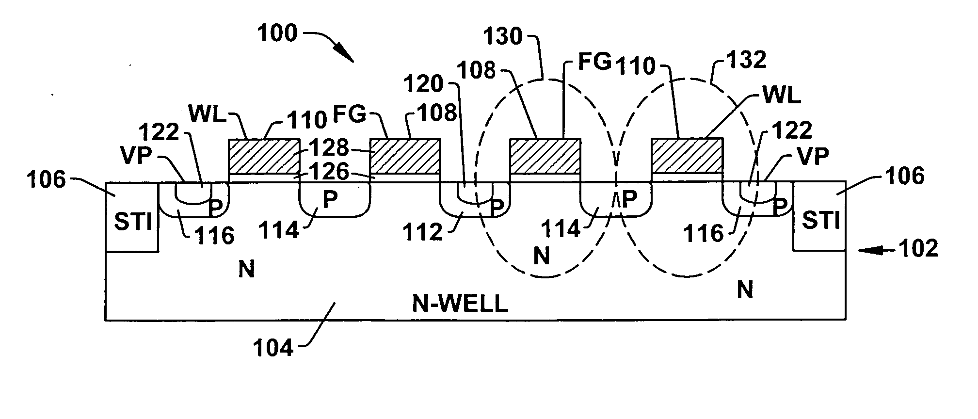
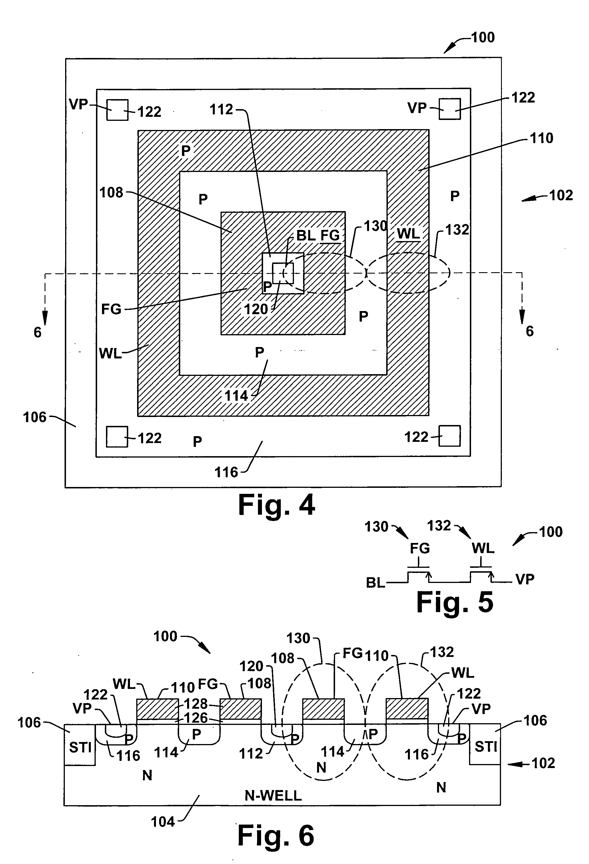
[0023] One or more aspects of the present invention are described with reference to the drawings, wherein like reference numerals are generally utilized to refer to like elements throughout, and wherein the various structures are not necessarily drawn to scale. In the following description, for purposes of explanation, numerous specific details are set forth in order to provide a thorough understanding of one or more aspects of the present invention. It may be evident, however, to one skilled in the art that one or more aspects of the present invention may be practiced with a lesser degree of these specific details. In other instances, well-known structures and devices are shown in block diagram form in order to facilitate describing one or more aspects of the present invention.

[0024] One or more aspects of the present invention pertain to forming a one time programmable (OTP) transistor based electrically programmable read only memory (EPROM) cell that lacks a conventional configu...


PUM


Abstract

The formation of a one time programmable (OTP) transistor based electrically programmable read only memory (EPROM) cell (100) is disclosed. The cell (100) includes multiple concentric rings (108, 110) out of which gate structures are formed. An inner transistor based cell (130) formed from the inner ring (108) is shielded from isolation material (106) by one or more outer rings (110). The lack of overlap between the inner transistor and any isolation material promotes enhanced charge/data retention by mitigating high electric fields that may develop at such overlap regions (30, 32).

Description

FIELD OF INVENTION [0001] The present invention relates generally to semiconductor devices and more particularly to forming a one time programmable (OTP) EPROM cell with improved data retention. BACKGROUND OF THE INVENTION [0002] One time programmable (OTP) electrically programmable read only memory (EPROM) can be an effective, low cost mechanism for providing non-volatile memory in a variety of computer related applications, such as in small handheld digital devices like cellular telephones, personal digital assistants (PDAs), etc. [0003] A one time programmable EPROM cell generally comprises a transistor that can be programmed once so that a particular amount of charge is stored within the cell, where the amount of charge stored within the cell corresponds to digital data (i.e., 0 or 1). An OTP transistor is programmed by applying a first known voltage to the cell, and the data stored within the cell is read basically by applying a second different voltage to the cell and reading ...

Claims


Application Information

Patent Timeline
Patent Type & Authority Applications(United States)
IPC IPC(8): H01L29/76
CPCH01L27/11206H01L27/112H10B20/20H10B20/00H01L29/788
Inventor WU, XIAOJU
Owner TEXAS INSTR INC
Why Eureka
Try Eureka