Semiconductor device and method of fabricating the same

a semiconductor device and semiconductor technology, applied in the field of semiconductor devices, can solve the problems of inhibiting the downsizing of semiconductor devices, widening the distance between electrodes, and worsening the forward current efficiency, so as to suppress the reverse leakage current

Inactive Publication Date: 2006-11-02
NEC ELECTRONICS CORP
View PDF8 Cites 52 Cited by
  • Summary
  • Abstract
  • Description
  • Claims
  • Application Information

AI Technical Summary

Benefits of technology

[0012] The second-conductivity-type region herein may be a guard ring region. In the present invention, the insulating film limits the position of the end portion of the metal electrode. This makes it possible to form the metal electrode at a desired position relative to the second-conductivity-type region and to the isolation insulating film. The metal electrode can be formed as being spaced from the isolation insulating film. This makes it possible to ensure a desirable Schottky contact between the metal electrode and the semiconductor substrate, without allowing the metal electrode to overlap the defect layer formed at the interface between the first-conductivity-type region and the isolation insulating film. It is also made possible to suppress defect-induced leakage current. In addition, the metal electrode can be formed so as to locate the end portion thereof on the second-conductivity-type region which serves as the guard ring. This makes it possible to further improve the Schottky contact between the metal electrode and the semiconductor substrate, and to effectively suppress the defect-induced leakage current. It is still also made possible to moderate concentration of electric field to the end portion of the metal electrode.
[0013] The insulating film and the metal electrode are provided in contact with each other, without placing any other constituents in between, raising an advantage of downsizing the semiconductor device. It is also made possible to improve current efficiency between the metal electrode and the opposing electrode, because the distance between these electrodes can be shortened.
[0014] In the present invention, the second-conductivity-type region and the isolation insulating film are kept distant from each other. In other words, the present invention can configure the semiconductor device so that a PN junction plane between the second-conductivity-type region and the first-conductivity-type region, differing in the conductivity type from each other, can be kept distant from the isolation insulating film. The distance between the second-conductivity-type region and the isolation insulating film can be determined, so that the depletion layer in a portion of the first-conductivity-type region between the second-conductivity-type region and the isolation insulating film, as being extended from the interface with the second-conductivity-type region, does not overlap the defect layer produced in the first-conductivity-type region along the interface thereof with the isolation insulating film. This makes it possible to suppress the reverse leakage current and therefore to realize a high-voltage Schottky barrier diode.
[0016] In this process, either of the step of forming the second-conductivity-type region and the step of forming the insulating film may precede the other. In the method of fabricating a semiconductor device, the metal electrode can be formed at a desired position using the insulating film as a mask. This makes it possible to form the metal electrode at a desired position relative to the second-conductivity-type region and the isolation insulating film.
[0017] The present invention can therefore suppress the reverse leakage current in the Schottky barrier diode, to thereby realize a high-voltage Schottky barrier diode.

Problems solved by technology

Wider distance between the electrodes worsens the forward current efficiency.
This worsens the forward current efficiency, and inhibits downsizing of the semiconductor device.
Growth of the depletion layer formed at the junction between the P-type guard ring 33 and the N-type semiconductor region 31 to as far as to overlap the defect layer will result in increase in reverse leakage current through the defect layer, and this makes it difficult to realize a high-voltage Schottky barrier diode.

Method used


Image

  • Semiconductor device and method of fabricating the same
  • Semiconductor device and method of fabricating the same
  • Semiconductor device and method of fabricating the same

Examples


first embodiment

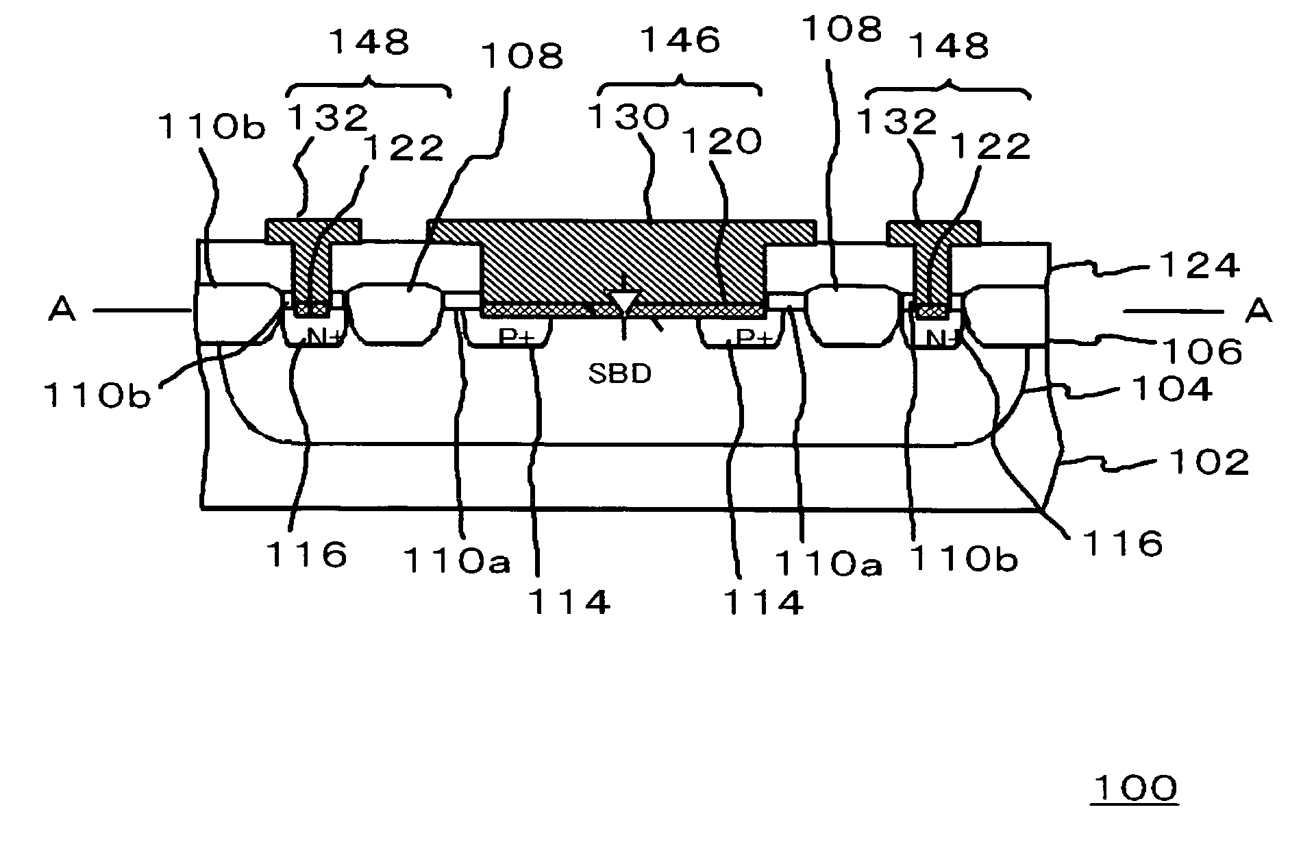
[0030]FIG. 1 is a sectional view showing a configuration of a semiconductor device of this embodiment.

[0031] A semiconductor device 100 has a semiconductor substrate 102 having a first-conductivity-type semiconductor region 104 (first-conductivity-type region) formed in the surficial portion thereof; an anode 146 (metal electrode) of a Schottky barrier diode formed on the first-conductivity-type semiconductor region 104; a second-conductivity-type guard ring 114 formed along the periphery of the anode 146 in the surficial portion of the first-conductivity-type semiconductor region 104, and; an isolation insulating film 108 formed along the periphery of, and being spaced from, the guard ring 114 in the surficial portion of the first-conductivity-type semiconductor region 104, so as to isolate the anode 146 from the other regions; and an anode-forming mask 110a covering the surface of the semiconductor substrate in a portion fallen between the anode 146 and the isolation insulating f...

second embodiment

[0064] This embodiment differs from the first embodiment in the configuration of the anode 146 and the cathode 148.

[0065]FIGS. 8A to 9B are sectional views showing process steps of fabricating a semiconductor device of this embodiment.

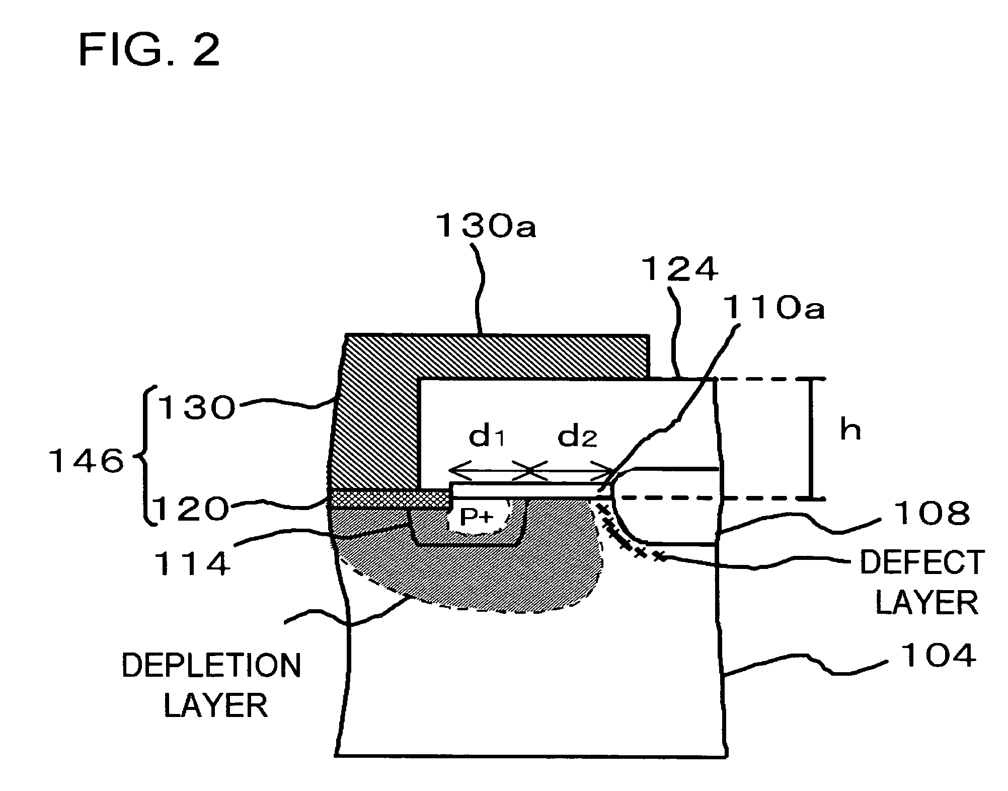
[0066] First, a structure configured as shown in FIG. 4B is formed according to the similar procedures as described in the first embodiment referring to FIGS. 4A and 4B. Next, the guard ring 114, which is a P+ layer, and the contact region 116, which is an N+ layer, are respectively formed by a photoresist process and ion implantation (FIG. 8A). The guard ring 114 herein is formed so as to ensure the above-described distance d2 between the outer end portion thereof and the end potion of the isolation insulating film 108, as described in the first embodiment. The guard ring 114 is formed also so as to allow the end portion of the anode-forming mask 110a to fall thereon. In other words, as shown in FIG. 2, the guard ring 114 is formed so as to overlap ...


PUM


Abstract

A semiconductor device 100 is configured as having a semiconductor substrate 102 having a first-conductivity-type semiconductor region 104 formed in its surficial portion; an anode 146 of a Schottky barrier diode formed on the first-conductivity-type semiconductor region 104; a second-conductivity-type guard ring 114 formed along the periphery of the anode 146 in the surficial portion of the first-conductivity-type semiconductor region; an isolation insulating film 108 formed along the periphery of, and being spaced from, the guard ring 114 in the surficial portion of the first-conductivity-type semiconductor region 104, so as to isolate the anode 146 from the other regions; and an anode-forming mask 110a covering the surface of the semiconductor substrate in a portion fallen between the anode 146 and the isolation insulating film 108, and being in contact with the end portion of the anode 146.

Description

[0001] This application is based on Japanese patent application No. 2005-131531 the content of which is incorporated hereinto by reference. BACKGROUND [0002] 1. Technical Field [0003] The present invention relates to a semiconductor device and a method of fabricating the same. [0004] 2. Related Art [0005] FIG. 11 is a sectional view showing a configuration of a semiconductor device described in Japanese Laid-Open Patent Publication No. H01-246873. The semiconductor device has a Schottky electrode 32 forming a Schottky diode on a first-conductivity-type (N-type) semiconductor region 31, and a guard ring 33 composed of a second-conductivity-type (P-type) impurity region around the Schottky diode. The semiconductor device herein further contains a doped semiconductor layer 34 provided in connection with the guard ring, and the doped semiconductor layer 34 is formed in contact with the Schottky electrode 32 of the Schottky barrier diode, so as to exclude any sidewall placed therebetween...

Claims


Application Information

Patent Timeline
Patent Type & Authority Applications(United States)
IPC IPC(8): H01L29/792
CPCH01L29/66136H01L29/872H01L29/8611H01L29/66143H01L31/108H01L31/10
Inventor SUDOU, JINSUKE
Owner NEC ELECTRONICS CORP
Why Eureka
Try Eureka