
Apparatus and method for controlling NAND flash memory

a technology of nand flash memory and controller, which is applied in the direction of lighting and heating equipment, instruments, carpet cleaners, etc., can solve the problems of increasing the complexity of data transmission control, difficult to realize a system on the chip (soc), and managing the buffer, so as to reduce the size of the memory chip and the time required to boot. , to achieve the effect of increasing data transmission speed

Inactive Publication Date: 2006-11-02
SAMSUNG ELECTRONICS CO LTD
View PDF6 Cites 45 Cited by
  • Summary
  • Abstract
  • Description
  • Claims
  • Application Information

AI Technical Summary

Benefits of technology

[0016] An aspect of the present invention provides an apparatus and method for controlling a NAND flash memory using a direct memory access (DMA) method, wherein the apparatus and method are capable of increasing data transmission speed, and reducing both memory chip size and the time required to boot a system.

Problems solved by technology

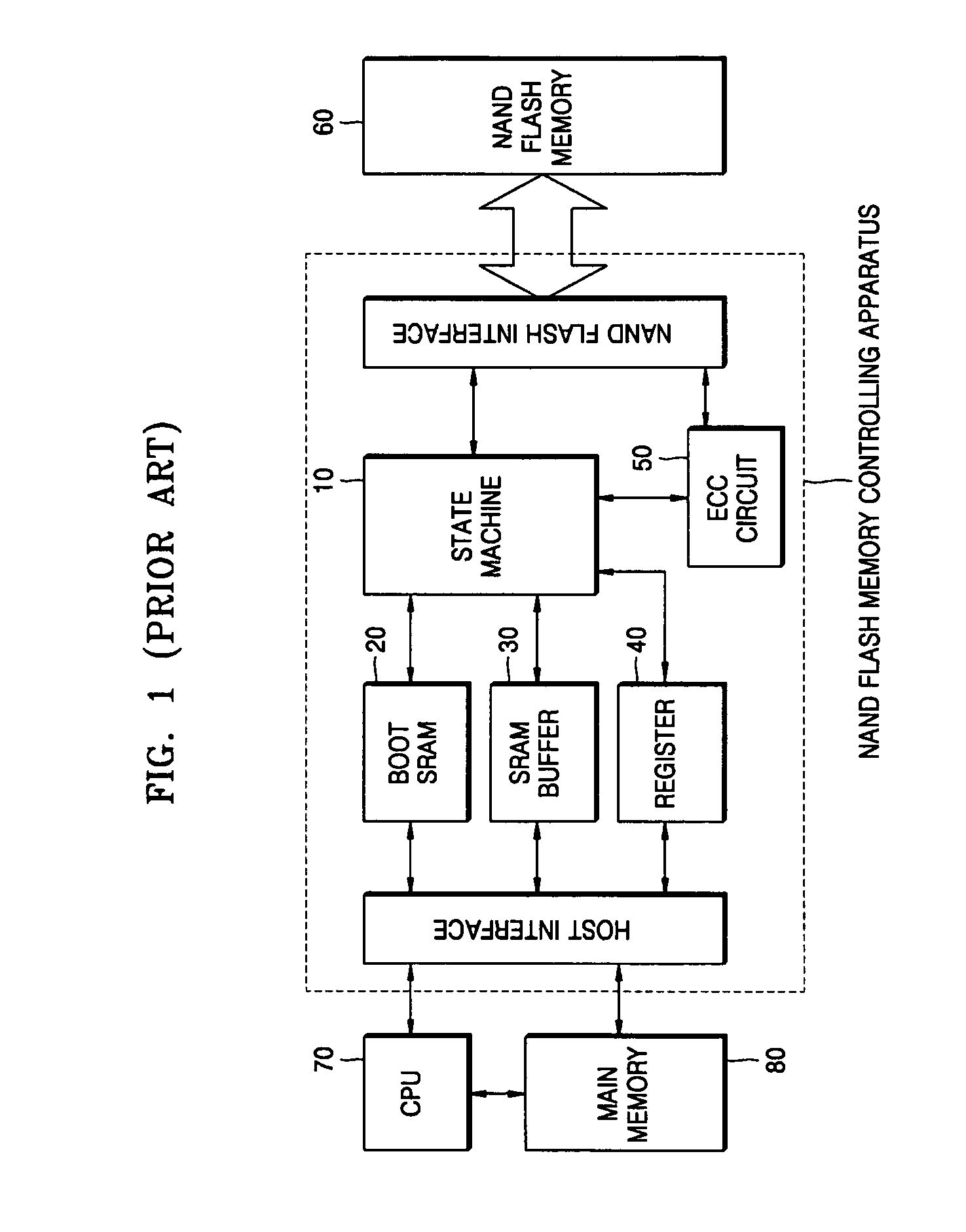
However, if a large capacity buffer is included in the NAND flash memory in order to improve speed of the NAND flash memory, managing the buffer is complicated, thus increasing the complexity of data transmission controlling.
Furthermore, as the size of the buffer is increased, a memory chip size increases, which makes it difficult to realize a system on chip (SoC).
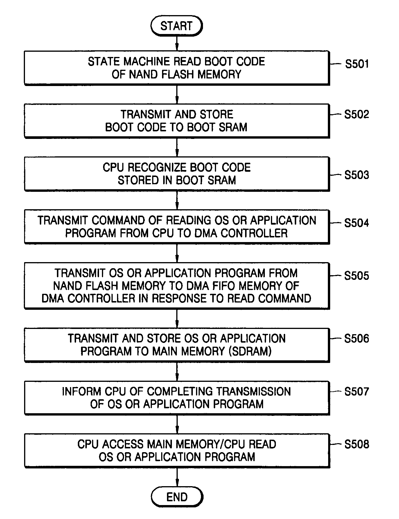
Moreover, according to the prior art, during system booting, since the OS code or application program code passes through the SRAM buffer and is transmitted to the main memory (SDRAM) in an operation of the CPU, it takes more time to boot.

Method used


Image

  • Apparatus and method for controlling NAND flash memory
  • Apparatus and method for controlling NAND flash memory
  • Apparatus and method for controlling NAND flash memory

Examples


Embodiment Construction

[0046] Reference will now be made in detail to the present embodiments of the present invention, examples of which are illustrated in the accompanying drawings, wherein like reference numerals refer to the like elements throughout. The embodiments are described below in order to explain the present invention by referring to the figures.

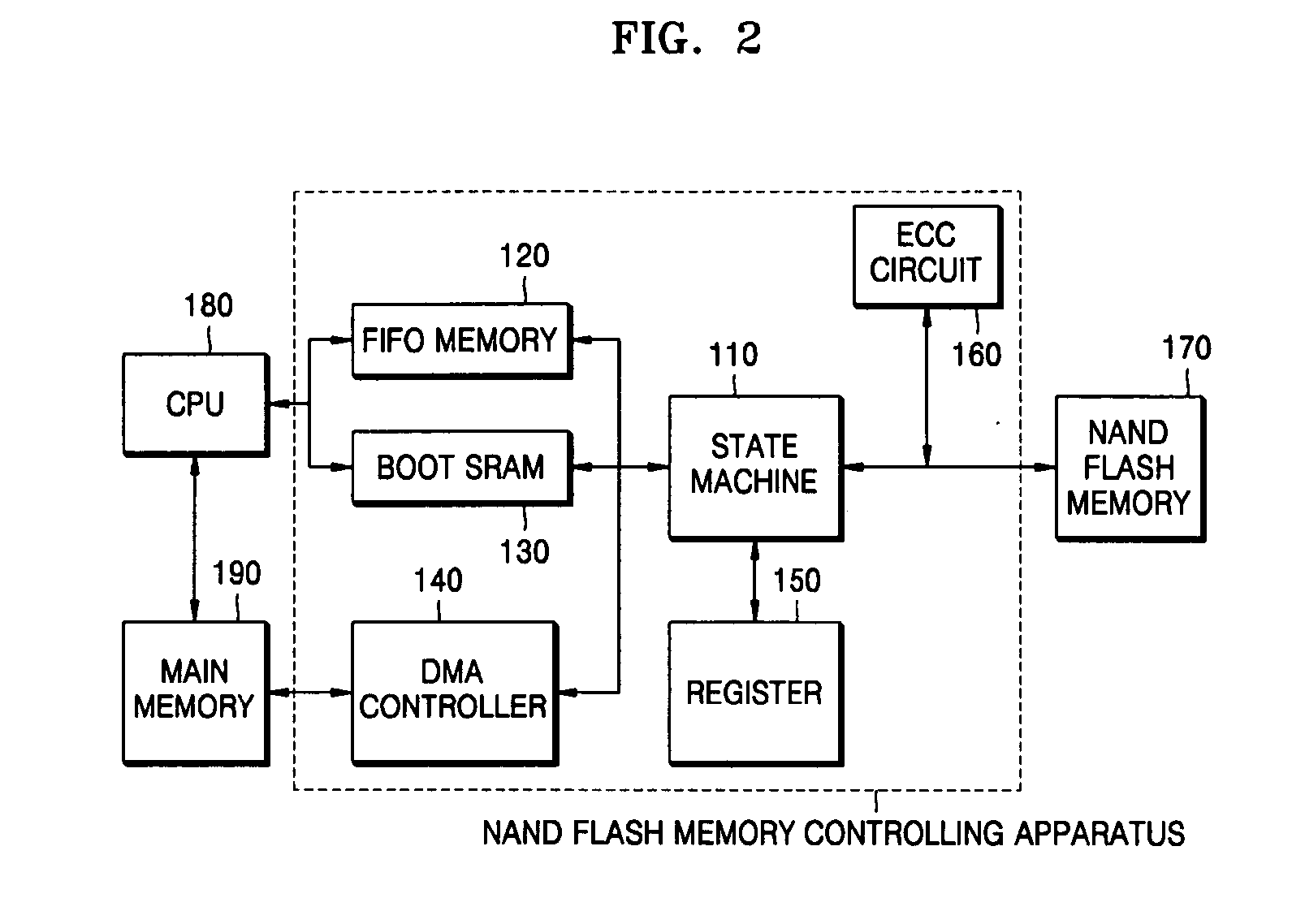
[0047]FIG. 2 is a block diagram schematically illustrating an apparatus for controlling a NAND flash memory according to an embodiment of the present invention. Referring to FIG. 2, the apparatus for controlling a NAND flash memory includes a state machine 110, a first-in first-out (FIFO) memory 120, a boot static random access memory (SRAM) 130, a direct memory access (DMA) controller 140, a register 150, and an error correction code (ECC) circuit 160. The apparatus for controlling a NAND flash memory interfaces with a NAND flash memory 170, a central processing unit (CPU) 180, and a main memory 190.

[0048] The state machine 110 controls operations ...


PUM


Abstract

An apparatus and method of controlling data transmission between a NAND flash memory and a central processing unit using a direct memory access (DMA) method. The apparatus includes: a register storing an operating command from the central processing unit and information related to the operating command; a boot memory storing a boot code for initializing a system; a direct memory access (DMA) controller transmitting data stored in the NAND flash memory to a main memory without passing through the central processing unit; and a state machine controlling the NAND flash memory controlling apparatus. Accordingly, data transmission speed is increased, chip memory size is decreased, and booting time is reduced.

Description

CROSS-REFERENCE TO RELATED APPLICATION [0001] This application claims the benefit of Korean Patent Application No. 10-2005-36528, filed on Apr. 30, 2005 in the Korean Intellectual Property Office, the disclosure of which is incorporated herein in its entirety by reference. BACKGROUND OF THE INVENTION [0002] 1. Field of the Invention [0003] An aspect of the present invention relates to an apparatus and method of controlling a NAND flash memory, and more particularly, to an apparatus and method of controlling data transmission between a NAND flash memory and a central processing unit (CPU) using a direct memory access (DMA) method. [0004] 2. Description of the Related Art [0005] A flash memory is a non-volatile memory device that can retain information stored therein even when a power supply is cut off, and is used as a mass storage device in portable devices such as digital cameras, MP3 players, mobile phones, or USB drivers. Flash memory is divided into NAND flash memory for data st...

Claims


Application Information

Patent Timeline
IPC IPC(8): G11C7/00
CPCG06F13/28G06F9/4403A47L11/20A47L11/4086A47L2601/04F22B1/284
Inventor CHOI, SANGIKPARK, HYANG-SUK
Owner SAMSUNG ELECTRONICS CO LTD
Learn More