Write once optical recording medium
- Summary
- Abstract
- Description
- Claims
- Application Information
AI Technical Summary
Benefits of technology
Problems solved by technology
Method used
Image
Examples
example 1
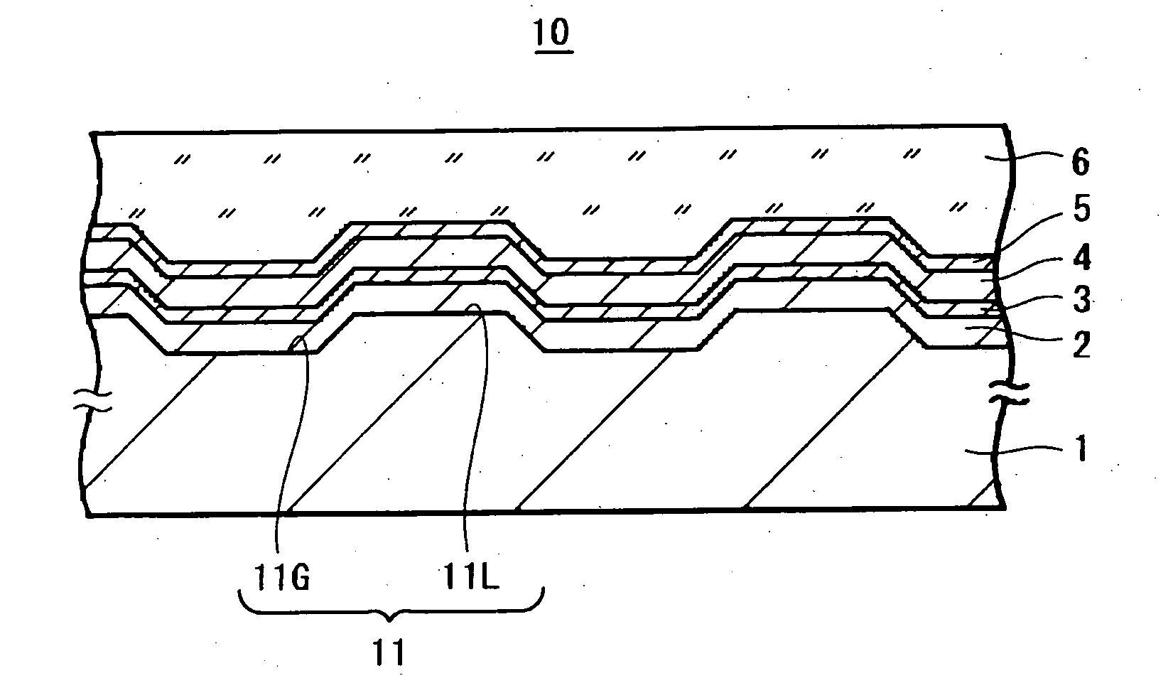
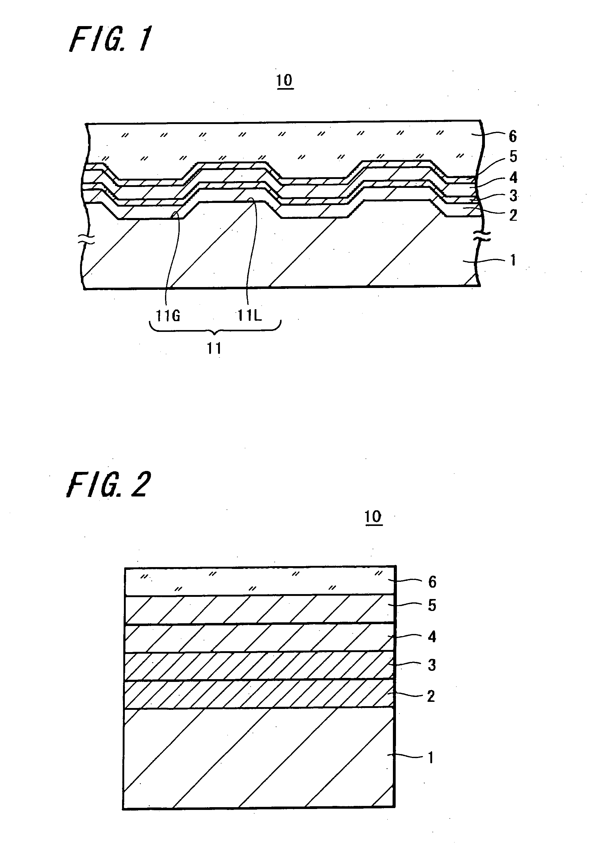
[0055]FIG. 2 is a diagram showing a film arrangement of a write once optical recording medium 10 in the inventive example 10.
[0056] In the write once optical recording medium 10 according to this inventive example 1, an uneven face 11 composed of grooves 11G and lands 11L was formed on a PC substrate 1 having a thickness of 1.1 mm as was already explained with reference to FIG. 1. A depth of this groove was 21 nm and a track pitch was 0.32 μm.
[0057] In the BD, the light illumination surface is the surface opposite to the opposite side of the substrate and a metal film 2 formed of an TiSi film having a thickness of 25 nm, a GeO oxide film 3 having a thickness of 22 nm, a first dielectric film 4 made of ZnS—SiO2 having a thickness of 45 nm and a second dielectric film 5 made of SiN having a thickness of 10 nm were sequentially deposited on the substrate 1. Then, a light transmission layer 6 was deposited on this second dielectric film 5. This light transmission layer 6 was formed by...
example 2
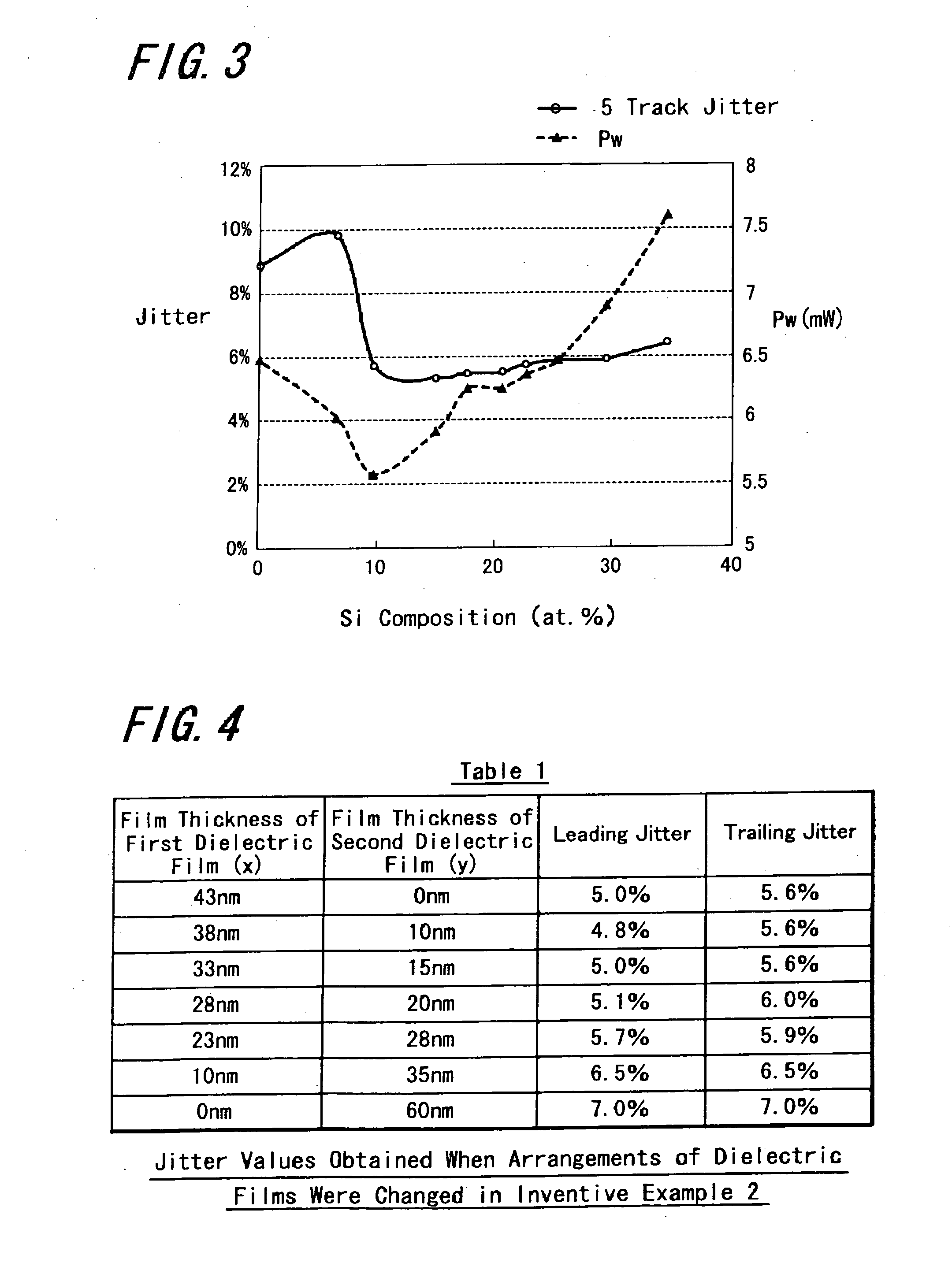
[0067] In the same arrangement as that of the inventive example 1, the film thickness of the first dielectric film was changed in a range of from 10 nm to 43 nm and the film thickness of the second dielectric film 5 was changed in a range of from 0 to 35 nm.
[0068] Then, the table 1 in FIG. 4 shows measured results of front end side jitter (leading jitter) and rear end side jitter of a recording mark obtained when the film thickness of the first dielectric film 4 was changed in a range of from 10 nm to 43 nm and the film thickness of the second dielectric film 5 was changed in a range of from 0 to 35 nm in the inventive example 2 and when the first dielectric film 4 is not provided and the film thickness of the second dielectric film 5 was selected to be 60 nm in the arrangement in the ranges other than this inventive example 2 for comparison.
[0069] A study of the measured results on the table 1 reveals that the leading jitter and the trailing jitter can be decreased to be less tha...
example 3
[0074] In this inventive example 3, as FIG. 5 shows its film arrangement, in the arrangement of the inventive example 1, the composition TiSi of the metal film 2, Si was selected to be 10 atomic %, the film thickness was selected to be 30 nm and the film thickness of the oxide film 3 was selected to be 10 nm.
[0075] Then, the film thickness of the first dielectric film 4 made of ZnS—SiO2 was selected to be 30 nm and the film thickness of the second dielectric film 5 made of SiN was selected to be 10 nm.
PUM
 Abstract
Description
Claims
Application Information


