Inter-digitated silicon photodiode based optical receiver on SOI

Inactive Publication Date: 2006-11-09
ANALOG DEVICES INC
View PDF6 Cites 9 Cited by
  • Summary
  • Abstract
  • Description
  • Claims
  • Application Information

AI Technical Summary

Problems solved by technology

These carriers effectively limit the speed of operation of photodiodes

Method used


Image

  • Inter-digitated silicon photodiode based optical receiver on SOI
  • Inter-digitated silicon photodiode based optical receiver on SOI
  • Inter-digitated silicon photodiode based optical receiver on SOI

Examples


Embodiment Construction

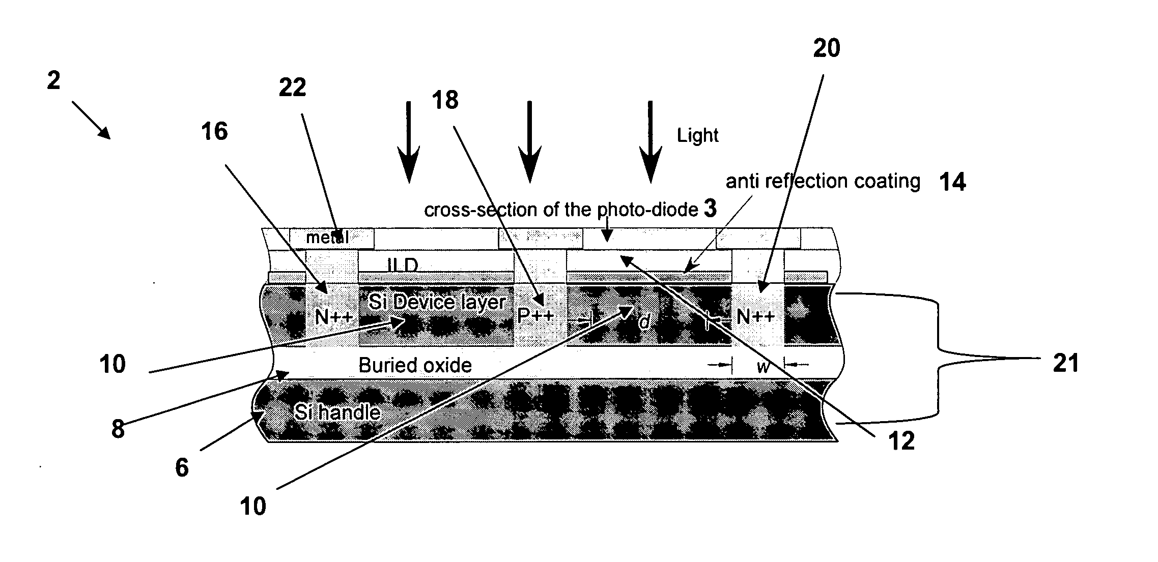
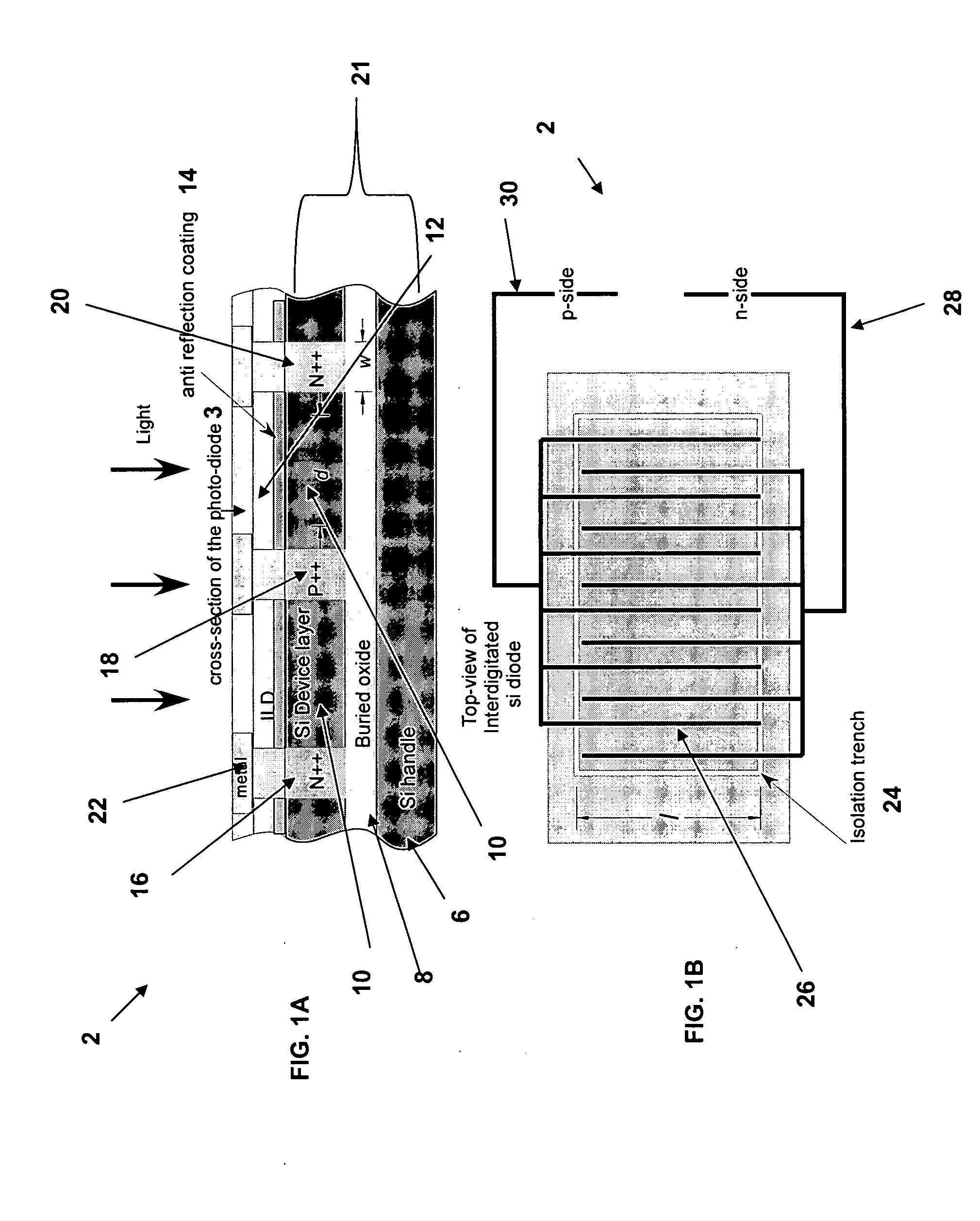
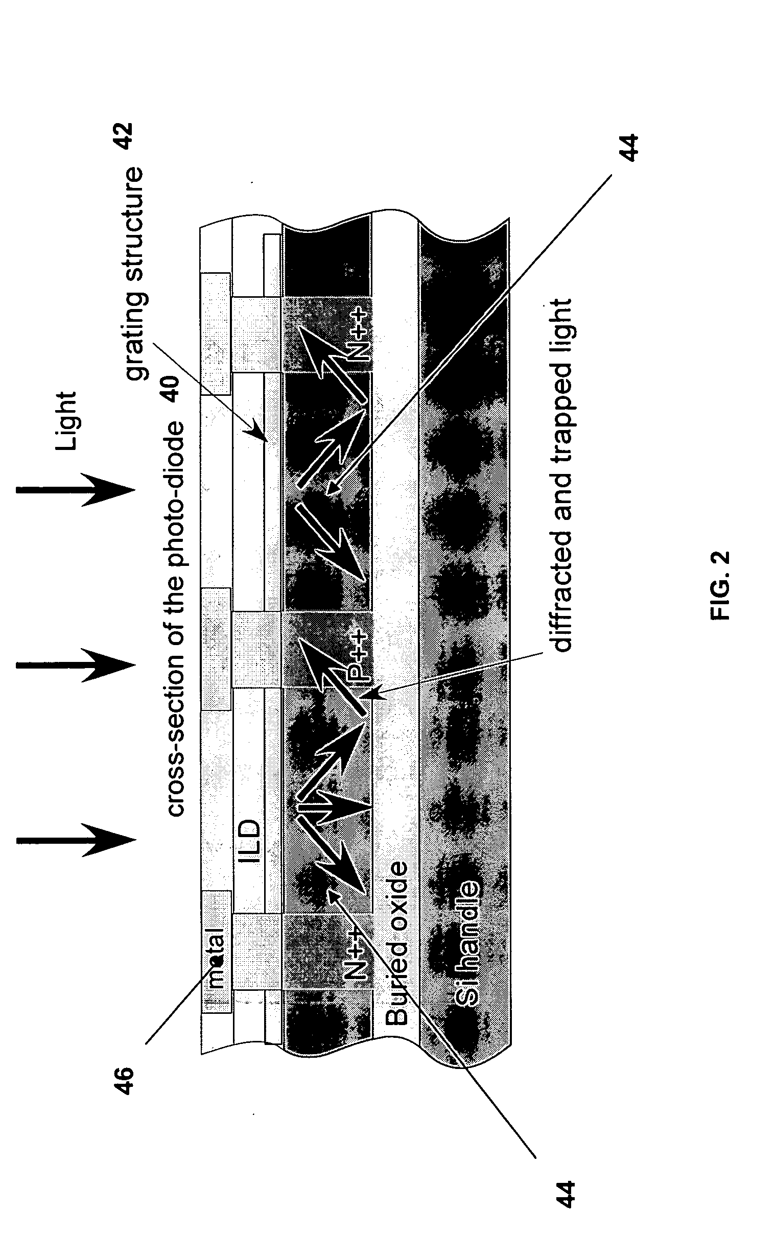
[0013] The invention involves an integrated silicon detector or integrated photo-receiver for high-speed data-oriented applications. The integration of silicon detectors with appropriate signal conditioning electronics is important in many high-volume applications. An inventive photo-detector geometry is provided that is compatible with high speed integrated signal conditioning electronics to allow us to use these detectors for many high-speed data oriented applications. In the present invention, photodiode is added to the high-speed Silicon-Germanium bipolar process on SOI to integrate high quality signal conditioning electronics with photodetector. This inventive integrated photodetector has many advantages over the known photodetectors. The signal conditioning electronics can include bipolar or CMOS transistors or any combination thereof. By integrating the photodetector and on-chip signal conditioning electronics, the performance of an optical receiver can be optimized.

[0014] M...


PUM


Abstract

A photodiode includes SOI substrate and a plurality of interdigitated electrodes comprising of different doped regions. A silicon device region is defined in the SOI substrate having a thickness between 0.5 and 5 microns.

Description

PRIORITY INFORMATION [0001] This application claims priority from provisional application Ser. No. 60 / 670,894 filed Apr. 13, 2005, which is incorporated herein by reference in its entirety.BACKGROUND OF THE INVENTION [0002] The invention relates to the field of photodetectors, and in particular to a photodetector compatible with high speed integrated signal conditioning electronics to allow for many high-speed data oriented applications. [0003] Silicon is a suitable semiconductor material for making optical photodetectors with wavelength range from ultraviolet to near infrared up to the band edge of silicon. Many detector structures and methods exist to make silicon detectors. [0004] Integrated silicon detectors are less common or almost absent in high speed communication systems such as gigabit Ethernet or storage area networks since these operate at wavelengths that are either weakly absorbed in silicon—850 nm with absorption depth of almost 22 μm—or where silicon is transparent—1...

Claims


Application Information

Patent Timeline
IPC IPC(8): H01L27/12
CPCH01L27/1443H01L31/0232H01L31/028Y02E10/547H01L31/101H01L31/103H01L31/03529H01L31/02327
Inventor DELIWALA, SHRENIK
Owner ANALOG DEVICES INC
Why Eureka
Try Eureka