Stacked type semiconductor device

a semiconductor memory device and stacking technology, applied in the field of stacking type semiconductor devices, can solve the problems of inability to use multi-layer circuit boards, stiffness and cost, and the effect of improving the noise immunity performance of semiconductor memory devices and increasing the efficiency of wiring efficiency and space usag

Inactive Publication Date: 2006-11-09
ELPIDA MEMORY INC
View PDF16 Cites 35 Cited by
  • Summary
  • Abstract
  • Description
  • Claims
  • Application Information

AI Technical Summary

Benefits of technology

[0024] As described above, according to the present invention, the stacked type semiconductor device is constructed by stacking the semiconductor chips on the baseboard, connecting between the pad row of each semiconductor chip and the terminal row of the baseboard with an interposer board having a plurality of wires with approximately the same length ar

Problems solved by technology

Construction of the semiconductor memory on a single semiconductor chip requires finer microfabrication as its capacity increases, and it is possible that the yield deteriorates.
However, when the interposer board is formed of, for example, a flexible board or the like, a multilayer circuit board cannot be used from the viewpoints of the low stiffness and cost, and it is difficult to achieve a wiring structure suita

Method used


Image

  • Stacked type semiconductor device
  • Stacked type semiconductor device
  • Stacked type semiconductor device

Examples


first embodiment

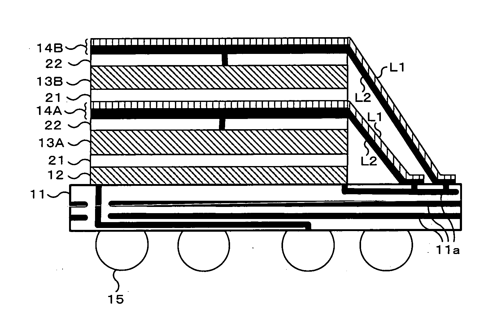
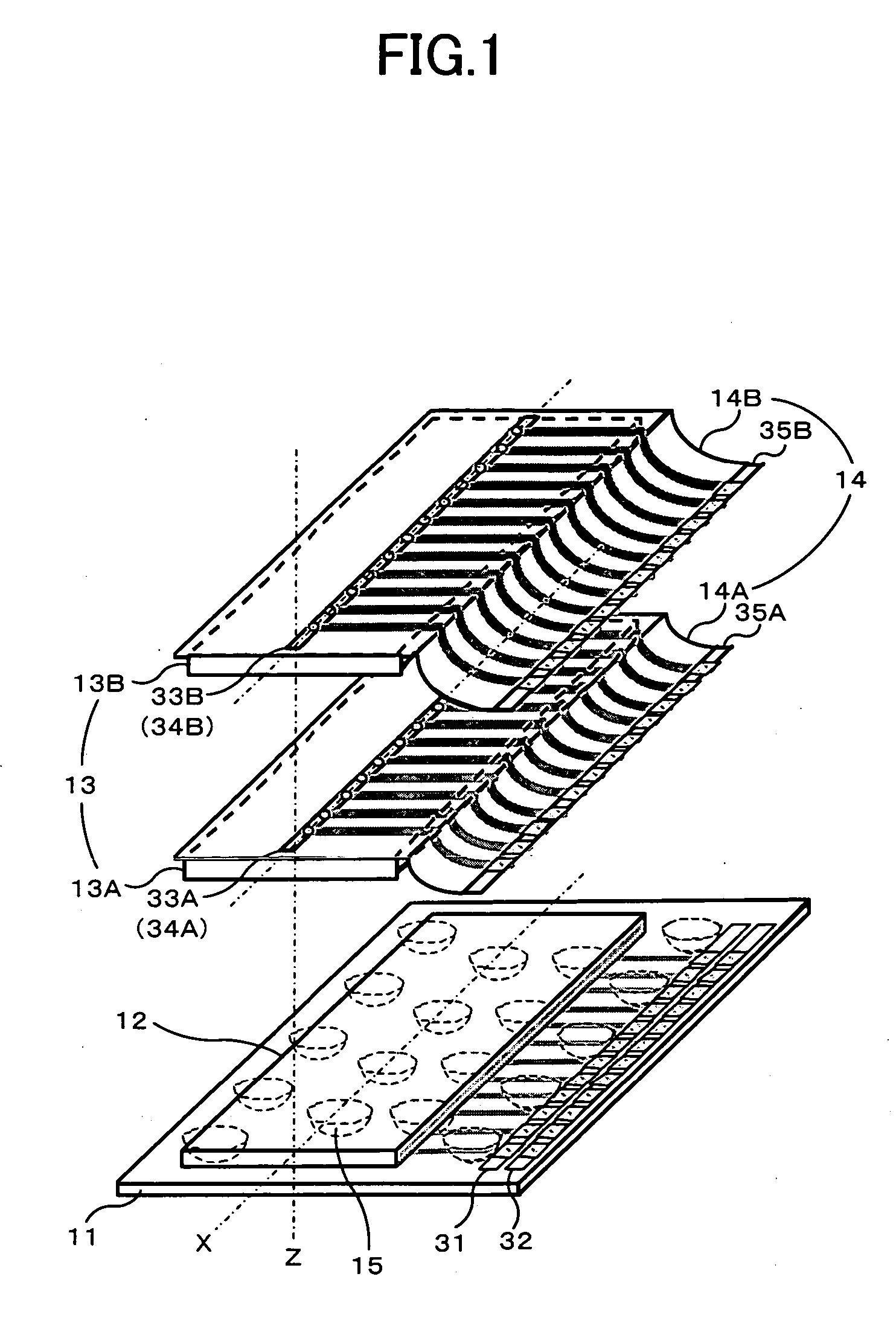
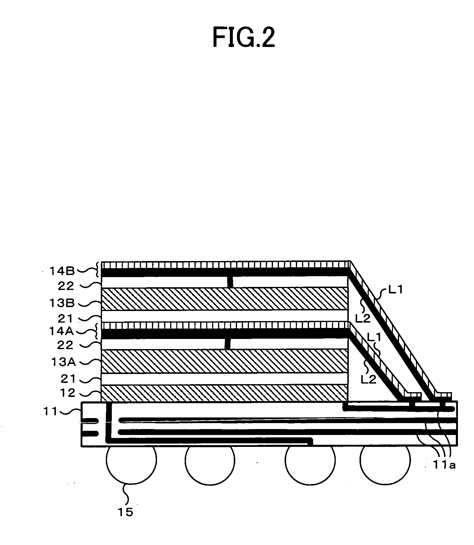
[0044] As shown in FIGS. 1 and 2, the stacked type memory of the first embodiment has a structure in which three semiconductor chips are stacked on the baseboard 11. The semiconductor chips to be stacked include an interface chip 12 for controlling input / output signals and two DRAM chips 13 each having a predetermined memory capacity in order from the bottom layer. And, two interposer boards 14 for making electrical connection between the DRAM chips 13 and the baseboard 11 are provided. The two DRAM chips 13 include a lower DRAM chip 13A and an upper DRAM chip 13B, and the two interposer boards 14 include an interposer board 14A connected to the lower DRAM chip 13A and an interposer board 14B connected to the upper DRAM chip 13B.

[0045] A number of solder balls 15 as external terminals used for connection to outside are attached to the bottom face of the baseboard 11. The baseboard 11 is a multilayer circuit board on which a wiring pattern 11a (FIG. 2) connected to the interface chip...

second embodiment

[0081] Next, the memory module using the stacked type memories of this embodiment will be described with reference to FIGS. 17 and 18. FIG. 17 shows a block diagram of the memory module composed of a memory controller MC and a plurality of stacked type memories M0 to M3. In FIG. 17, for example, the stacked type memory M2 is constructed shown in FIG. 5 and includes the interface chip 12 and four DRAM chips 13. The other stacked type memories M0, M1 and M3 may have the same configuration as the stacked type memory M2 or may have different configuration from each other. The memory controller MC controls operations of the stacked type memories M0 TO M3 through the bus, so that the entire memory module functions as a single large capacity memory. As an example of the appearance of the memory module having the configuration of FIG. 17, FIG. 18A shows a plane view and FIG. 18B shows a side view. In this manner, a thin memory module having a number of external terminals can be constructed...


PUM


Abstract

A stacked type semiconductor device comprising: a baseboard having a terminal row formed at an end in which connecting terminals is arranged linearly and having a wiring pattern connected to the connecting terminals and external terminals; semiconductor chips having a pad row in which pads is arranged linearly in parallel to the terminal row and being stacked on the baseboard; and interposer boards having a wiring layer including a plurality of wires arranged in parallel with the same length for connecting between pads of the pad row and connecting terminals of the terminal row.

Description

BACKGROUND OF THE INVENTION [0001] 1. Field of the Invention [0002] The present invention relates to a technical field of a stacked type semiconductor device having a structure in which a plurality of semiconductor chips is arranged. [0003] 2. Description of the Related Art [0004] In recent years, a further increase in the capacity of a semiconductor memory such as DRAM has been demanded in order to achieve higher performance of apparatuses. Construction of the semiconductor memory on a single semiconductor chip requires finer microfabrication as its capacity increases, and it is possible that the yield deteriorates. Thus, a stacked type semiconductor device having a structure in which a plurality of semiconductor chips is stacked on a baseboard has been proposed. For example, by stacking a plurality of DRAM chips and an interface chip for controlling data input / output of each DRAM chip on the baseboard, a stacked type memory with a small size and large capacity capable of being con...

Claims


Application Information

Patent Timeline
IPC IPC(8): H01L23/02
CPCH01L24/50H01L25/0657H01L2225/06527H01L2225/06551H01L2225/06579H01L2924/01023H01L2924/01082H01L2924/15311H01L2924/3011H01L2924/01005H01L2924/01006H01L2924/01033A01D23/04
Inventor KATAGIRI, MITSUAKISHIBAMOTO, MASANORIHARA, TSUTOMUAOKI, KOICHIROKANDA, NAOYAKIKUCHI, SHUJITANIE, HISASHI
Owner ELPIDA MEMORY INC
Why Eureka
Try Eureka