
FPGA emulation system

a programmable gate array and emulation system technology, applied in the field of improved field programmable gate array (fpga) emulation system, can solve the problems of slow logic simulator when compared to the speed of an fpga, inability to model the constraints imposed by the physical structure of a typical fpga, and inability to justify the cost of developing a custom silicon device when compared to the cost of using an fpga,

Inactive Publication Date: 2006-11-09
ALTERA CORP
View PDF22 Cites 31 Cited by
  • Summary
  • Abstract
  • Description
  • Claims
  • Application Information

AI Technical Summary

Benefits of technology

[0016] It is a further object of this invention to provide such an FPGA emulation system which enables testing of FPGA designs in their native operating environment prior to completing the design of the components of the FPGA.
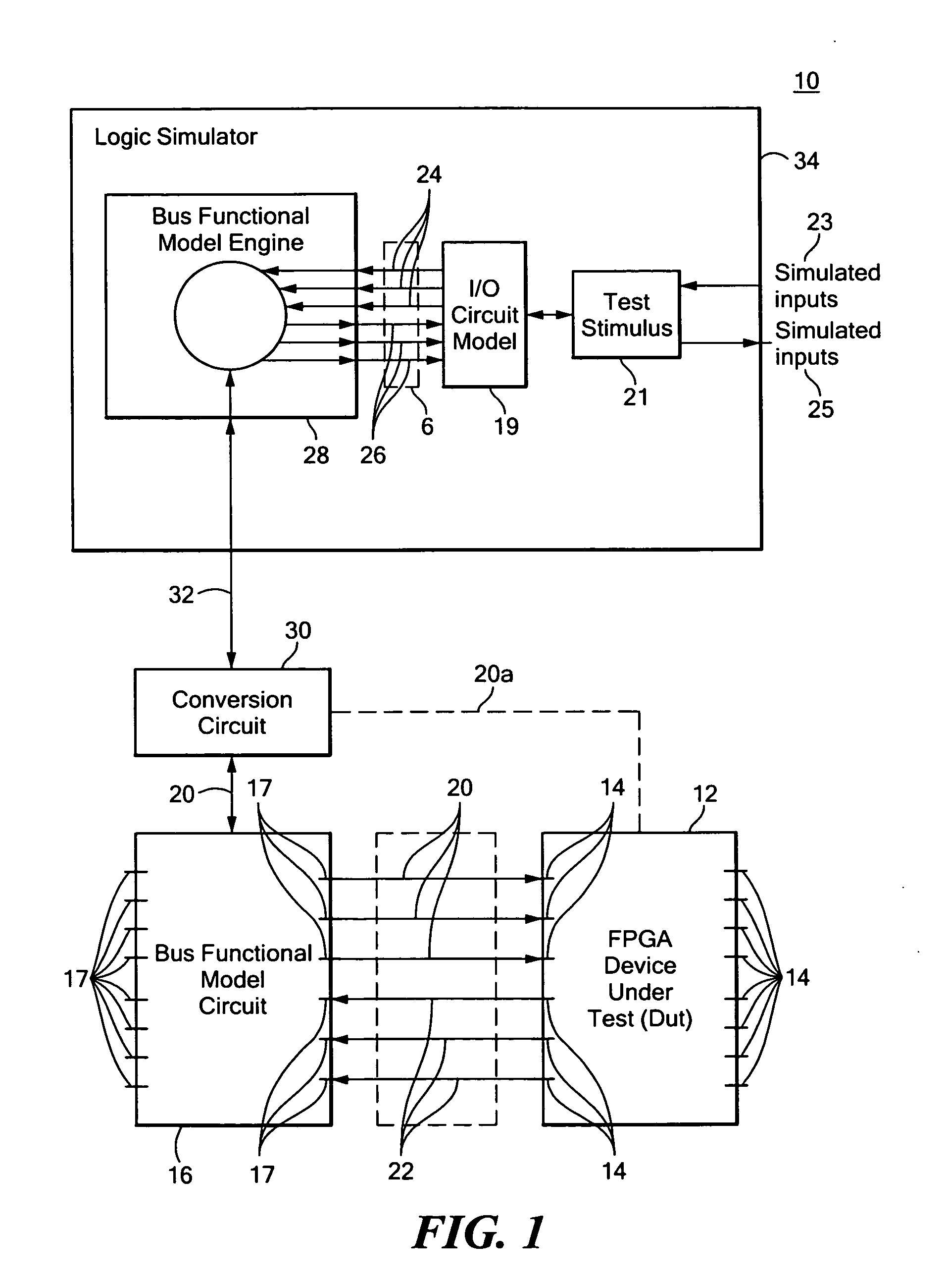
[0037] This invention further features an FPGA emulation system including an FPGA device under test having a plurality of pins, a bus functional model circuit having a plurality pins, a connector coupling the FPGA device under test to the bus functional model circuit, and wherein the bus functional model circuit is programmed to input signals into the FPGA device under test and to receive output signals from the FPGA device under test to more accurately emulate the operation of the FPGA device under test in a predefined selectable and flexible electrical operating environment.

Problems solved by technology

In this case, the expense associated with developing a custom silicon device is not justified when compared to the cost of using an FPGA with customized logic.
However, logic simulators are slow when compared to the speed of an FPGA.
Logic simulators also cannot model the constraints imposed by the physical structure of a typical FPGA, such as package pin functions, and the like.
Hence, logic emulators provide no new information over logic simulators and cannot determine whether a logic design will fit within a specific FPGA or if the FPGA will operate at the desired speed of the target system.
By definition, prototype boards are considered flawed.
Errors involving the pinout configuration of the FPGA typically cannot be repaired without re-building the entire prototype board.
Errors related to the power supplies of the FPGA may result in a non-functional board.
Errors in configuration and programming interfaces often result in an FPGA that cannot be programmed on the prototype board.
Prototype boards are also very expensive and time consuming to build.
One problem with evaluation boards is that the FPGA design typically has to be modified or tailored to fit on an existing evaluation board.
In other cases, the evaluation board may have the desired FPGA device but it is not mounted in the desired device package.
The result is the evaluation board may not provide information about the validity of pinout configurations of the target FPGA design.
Any changes to the target FPGA design have the potential to prevent detection of errors in the design, or may introduce new errors, in the target FPGA design, rendering the modeling effort useless.
Conventional emulation systems and logic simulators also provide no way to emulate and verify the internal operation of the various components within an FPGA in the actual target environment of the FPGA using software.
Thus, the operation of design components inside the FPGA can only be tested apart from the external components they are intended to communicate with.
However, electrical communication with an emulator prohibits high speed communication between the emulated FPGA design and the native environment.
Testing of actual FPGA circuits at the speed they are intended to operate in their native operating environment typically cannot be achieved with conventional emulation systems and logic simulators.
Conventional logic simulators and emulation systems often provide inaccurate system models, inaccurate FPGA circuit models, and inaccurate design translation software.
In practice, this translation process is imperfect, resulting in differences between design function in simulation or emulation and in the native operating environment of the FPGA device.
In practice, these models and the circuits they model are imperfect and functional differences result between logic simulation or emulation and actual FPGA designs.
In practice, these models are not as accurate as the elements they model in the actual FPGA components.
This mapping difference results in functional differences between the simulated or emulated designs and the actual FPGA designs.

Method used


Image

  • FPGA emulation system
  • FPGA emulation system
  • FPGA emulation system

Examples


Embodiment Construction

[0054] Aside from the preferred embodiment or embodiments disclosed below, this invention is capable of other embodiments and of being practiced or being carried out in various ways. Thus, it is to be understood that the invention is not limited in its application to the details of construction and the arrangements of components set forth in the following description or illustrated in the drawings. If only one embodiment is described herein, the claims hereof are not to be limited to that embodiment. Moreover, the claims hereof are not to be read restrictively unless there is clear and convincing evidence manifesting a certain exclusion, restriction, or disclaimer.

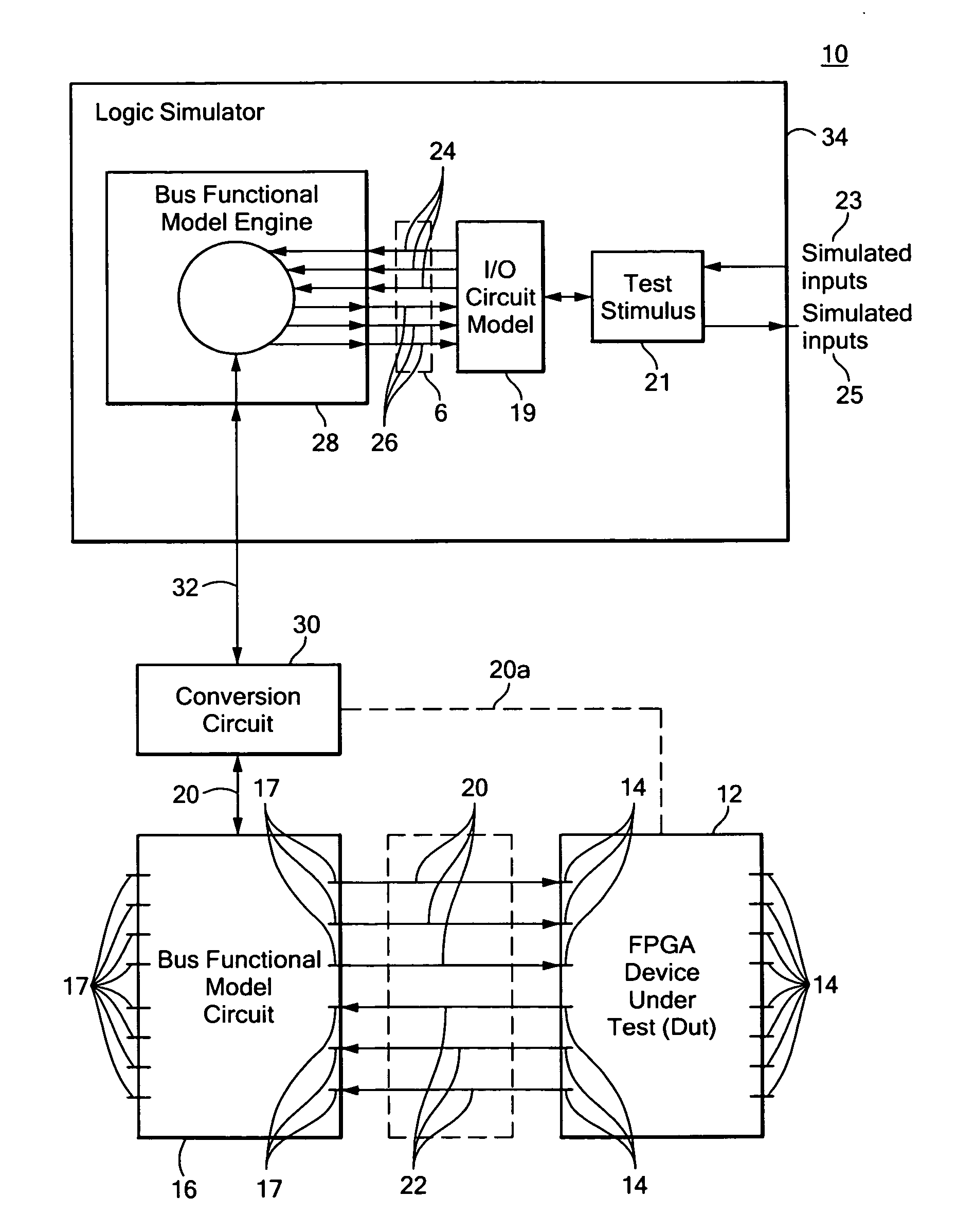
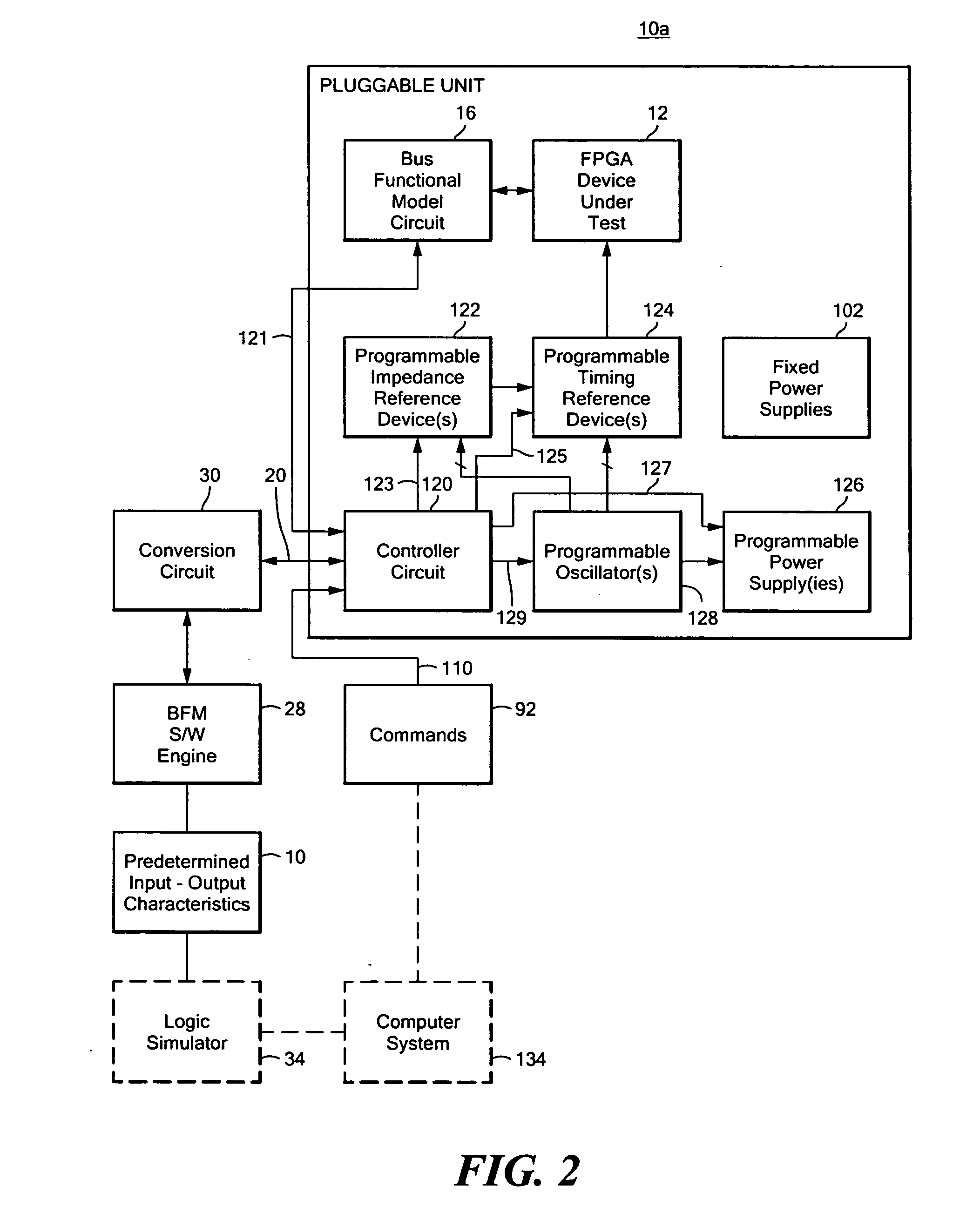
[0055] There is shown in FIG. 1, FPGA emulation system 10 of this invention including an FPGA device under test 12 having plurality of pins 14. As discussed in the Background section above, FPGA device under test 12 is an FPGA device that is often used to model and verify a custom logic design before production of a silic...


PUM


Abstract

This invention features an FPGA emulation system including an FPGA device under test having a plurality of pins. A bus functional model circuit responsive to signals representing predetermined input characteristics of the FPGA device under test and configured to apply one or more signals to the FPGA device under test corresponding to the predetermined input characteristics and configured to receive one or more signals representing output characteristics of the FPGA device under test to emulate the operation of the FPGA device under test in a predefined selectable and flexible electrical operating environment. This invention also features an FPGA emulation system including an FPGA device under test having at least one component and a plurality of pins operating in a predetermined native target environment, a bus functional model engine for simulating and capturing output characteristics of the at least one component of the FPGA device under test and simulating and releasing input characteristics of the at least one component of the FPGA device under test, and a bus functional model circuit embedded in the FPGA device under test configured to receive one or more signals representing the input characteristics of the at least one component and configured to release one or more signals representing the output characteristics of the at least one component such that the bus functional model engine emulates the operation of the at least one component of the FPGA device under test in the predetermined native target environment.

Description

RELATED APPLICATIONS [0001] This application claims benefit of U.S. Provisional Application Ser. No. 60 / 662,427, filed on Mar. 16, 2005, entitled “Scalable FPGA Emulation System”, hereby incorporated herein by reference.FIELD OF THE INVENTION [0002] This invention relates to an improved field programmable gate array (FPGA) emulation system that emulates the operation of an FPGA design in a selectable and flexible electrical operating environment. BACKGROUND OF THE INVENTION [0003] An FPGA is often used to prototype logic designs for custom silicon devices such as ASICs, and the like. Because an FPGA is less expensive and typically takes less time to develop than an ASIC or similar device, the logic design intended for an ASIC is often ported to an FPGA for evaluation prior to committing it to production. An FPGA may also be included in the design of a final product that does not need the high performance, low cost or design capacity of an ASIC. In this case, the expense associated w...

Claims


Application Information

Patent Timeline
Patent Type & Authority Applications(United States)
IPC IPC(8): G01R31/28G06F11/00
CPCG01R31/31704G06F17/5027G06F11/261G01R31/318519G06F30/331
Inventor SCHALICK, CHRISTOPHER A.
Owner ALTERA CORP
Learn More