Elimination of gate oxide weak spot in deep trench

a technology of gate oxide and deep trench, which is applied in the field of cell structure and fabrication process of semiconductor devices, can solve the problems of weak spots formed around the corners of the trench bottom, difficulty in forming thick oxide layers at the bottom of the trench, and often become obstacles, so as to improve device reliability, eliminate or reduce malfunctions, and improve device reliability

Inactive Publication Date: 2006-11-16
M MOS SEMICON
View PDF10 Cites 14 Cited by
  • Summary
  • Abstract
  • Description
  • Claims
  • Application Information

AI Technical Summary

Benefits of technology

[0010] Specifically, it is an object of the present invention to provide a different and novel trench structure and fabrication process for a semiconductor power device wherein the weak spots of the oxide layer is protected by a composite oxide such that the device reliability may be improved by eliminating or reducing the malfunctions caused by the weak spots on the gate oxide.
[0011] Another object of the present invention is to provide a different and novel trench structure and fabrication process for a semiconductor power device wherein the deposition of the oxide layer is performed before the deposition of the thick bottom insulator layer. Furthermore, the gate oxide is protected by an etch stop layer to prevent development of oxide weak spots on the oxide layer such that the device reliability may be improved.

Problems solved by technology

For those with ordinary skill in the art of semiconductor manufacture, there is still a technical difficulty in forming a thick oxide layer at the bottom of a trench opened in a semiconductor substrate.
Specifically, in the process of forming a thick oxide layer at the bottom of a deep trench with a narrow trench critical dimension (CD), inevitably there are weak spots formed around the corners of the trench bottom.
This technical difficulty often becomes a hindrance to implement a semiconductor device for high switching speed operation.
However, due to the concern of the weak interface spots between the thick oxide bottom layer and the linen layer on the sidewalls, the reliability of semiconductor devices is adversely affected.
However, the layer interfaces disposed near the corner of the trench bottom all have the weak spots that could develop into reliability problems during the life cycles of the device operation.
At these interface points, the gate oxide layer growth is limited due to restricted oxygen diffusion into the corner interface.
These weak points often leads to device reliability problems and may further adversely affect the device performance.

Method used


Image

  • Elimination of gate oxide weak spot in deep trench
  • Elimination of gate oxide weak spot in deep trench
  • Elimination of gate oxide weak spot in deep trench

Examples


Embodiment Construction

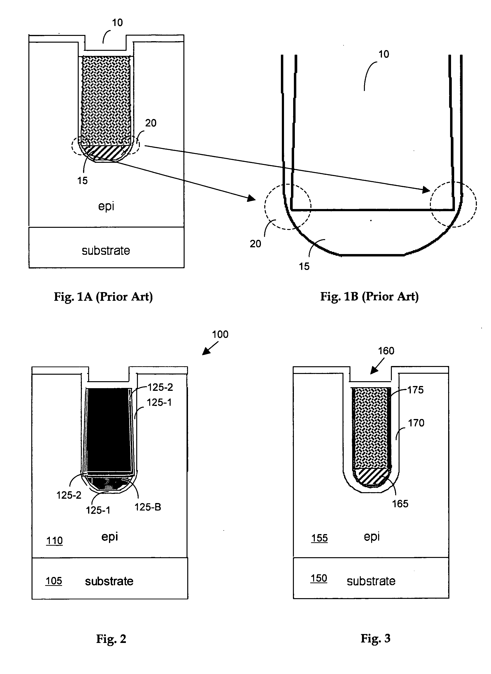
[0019] Please refer to FIG. 2 for a first preferred embodiment of this invention where a semiconductor device 100 is supported on a substrate 105 formed with an epitaxial layer 110. The semiconductor device 100 includes a trench 115 generally filled with polysilicon 120 to function as a gate. For the purpose of eliminating the weak oxide spots, the trenched gate 120 includes a composite dual gate oxide layer 125-1 and 125-2. The first oxide layer 125-1 is first formed for covering the sidewalls and the bottom of the trench 115 with a thick oxide layer 125-B disposed on the bottom of the trench. Then a second oxide layer 125-2 is formed that is disposed on top of the first oxide layer 125-1 and the thick bottom oxide layer 125-B. The second oxide layer 125-2 is formed to fill the weak oxide spots at the corner of the trench bottom. With a dual composite oxide layer, i.e., layers 125-1 and 125-2, the weak spots at the bottom corners of the trench are eliminated.

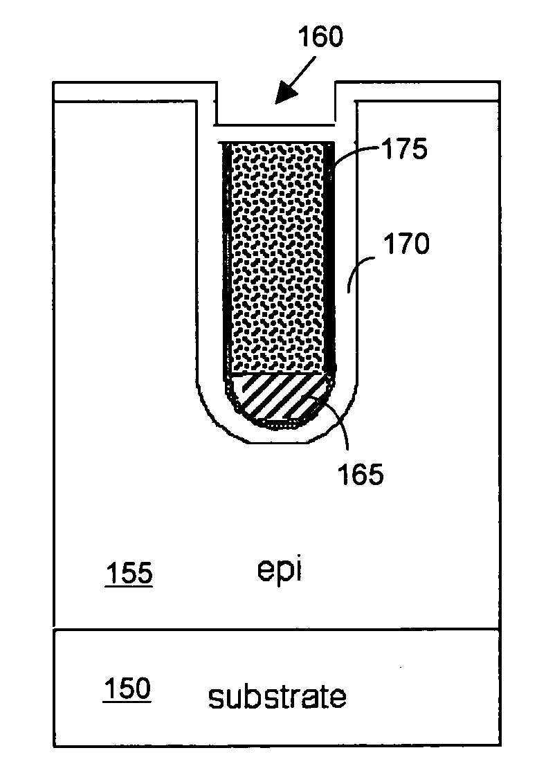
[0020]FIG. 3 shows ano...


PUM


Abstract

A MOSFET with a 0.7˜2.0 micrometers deep trench is formed by first carrying out a processing step of opening a trench in a semiconductor substrate. A thick insulator layer is then deposited in the trench such that the film at the bottom of the trench is much thicker than the sidewall of the trench. The insulator layer at the sidewall is then removed followed by the creation of composite dual layers that form the Gate Oxide. Another embodiment has the insulator layer deposited after Gate Oxide growth and stop at a thin Nitride layer which serves as stop layer during insulator pullback at trench sidewall and during Polysilicon CMP. Embodiments of the present invention eliminates weak spot at trench bottom corner encountered when Gate Oxide is grown in a 0.2 micrometers deep trench with thick bottom oxide. The present invention also maintains good control of the shape of the trench and the thickness profile of the Gate Oxide

Description

BACKGROUND OF THE INVENTION [0001] 1. Field of the Invention [0002] This invention relates generally to the cell structure and fabrication process of semiconductor devices. More particularly, this invention relates to a novel and improved cell structure and improved process for fabricating a trenched semiconductor device, e.g., a trenched power MOSFET device, to eliminate gate oxide weak spot in a deep trench. [0003] 2. Description of the Prior Art [0004] For those with ordinary skill in the art of semiconductor manufacture, there is still a technical difficulty in forming a thick oxide layer at the bottom of a trench opened in a semiconductor substrate. Specifically, in the process of forming a thick oxide layer at the bottom of a deep trench with a narrow trench critical dimension (CD), inevitably there are weak spots formed around the corners of the trench bottom. Particularly, these spots are developed at the points where the curvature of the surfaces of the insulator and silico...

Claims


Application Information

Patent Timeline
Patent Type & Authority Applications(United States)
IPC IPC(8): H01L29/94
CPCH01L21/28185H01L29/66621H01L29/512H01L21/28194
Inventor HSHIEH, FWU-IUANFAI, YEE AIKEONG, NG YEOW
Owner M MOS SEMICON
Why Eureka
Try Eureka