
Silicon carbide junction barrier schottky diodes with supressed minority carrier injection

a silicon carbide junction barrier and minority carrier technology, applied in the field of diodes, can solve the problems of inability to achieve device may not exhibit significant reverse recovery charge and reverse recovery time, and the device may not be able to conduct curren

Active Publication Date: 2006-11-16
CREE INC
View PDF6 Cites 127 Cited by
  • Summary
  • Abstract
  • Description
  • Claims
  • Application Information

AI Technical Summary

Problems solved by technology

Silicon-based PIN devices typically exhibit relatively poor switching speeds.
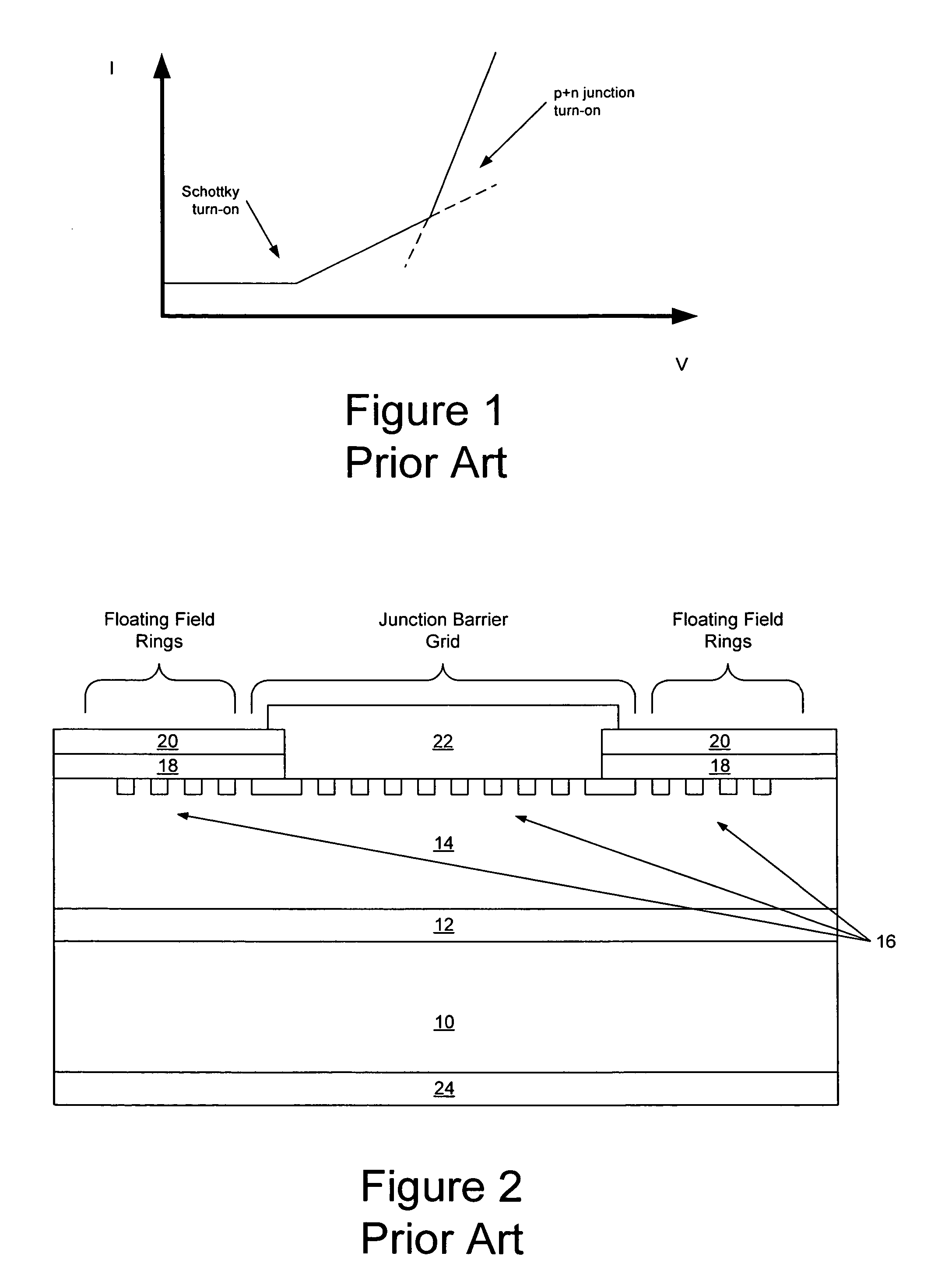
Since the drift layer of the diode is flooded with carriers, the device may show significant reverse recovery charge and reverse recovery time.
Thus, when such a device is switched from the forward bias (conducting) state to the reverse bias (blocking) state, it would undesirably continue to conduct current until all injected minority carriers have recombined.
In addition, carrier recombination can cause propagation of stacking faults, which may result in severe degradation of the I-V characteristics.

Method used


Image

  • Silicon carbide junction barrier schottky diodes with supressed minority carrier injection
  • Silicon carbide junction barrier schottky diodes with supressed minority carrier injection
  • Silicon carbide junction barrier schottky diodes with supressed minority carrier injection

Examples


Embodiment Construction

[0040] The present invention now will be described more fully hereinafter with reference to the accompanying drawings, in which embodiments of the invention are shown. However, this invention should not be construed as limited to the embodiments set forth herein. Rather, these embodiments are provided so that this disclosure will be thorough and complete, and will fully convey the scope of the invention to those skilled in the art. In the drawings, the thickness of layers and regions are exaggerated for clarity. Like numbers refer to like elements throughout. As used herein the term “and / or” includes any and all combinations of one or more of the associated listed items.

[0041] The terminology used herein is for the purpose of describing particular embodiments only and is not intended to be limiting of the invention. As used herein, the singular forms “a”, “an” and “the” are intended to include the plural forms as well, unless the context clearly indicates otherwise. It will be furt...


PUM

PropertyMeasurementUnit
thickaaaaaaaaaa
thickaaaaaaaaaa
carrier concentrationaaaaaaaaaa

Abstract

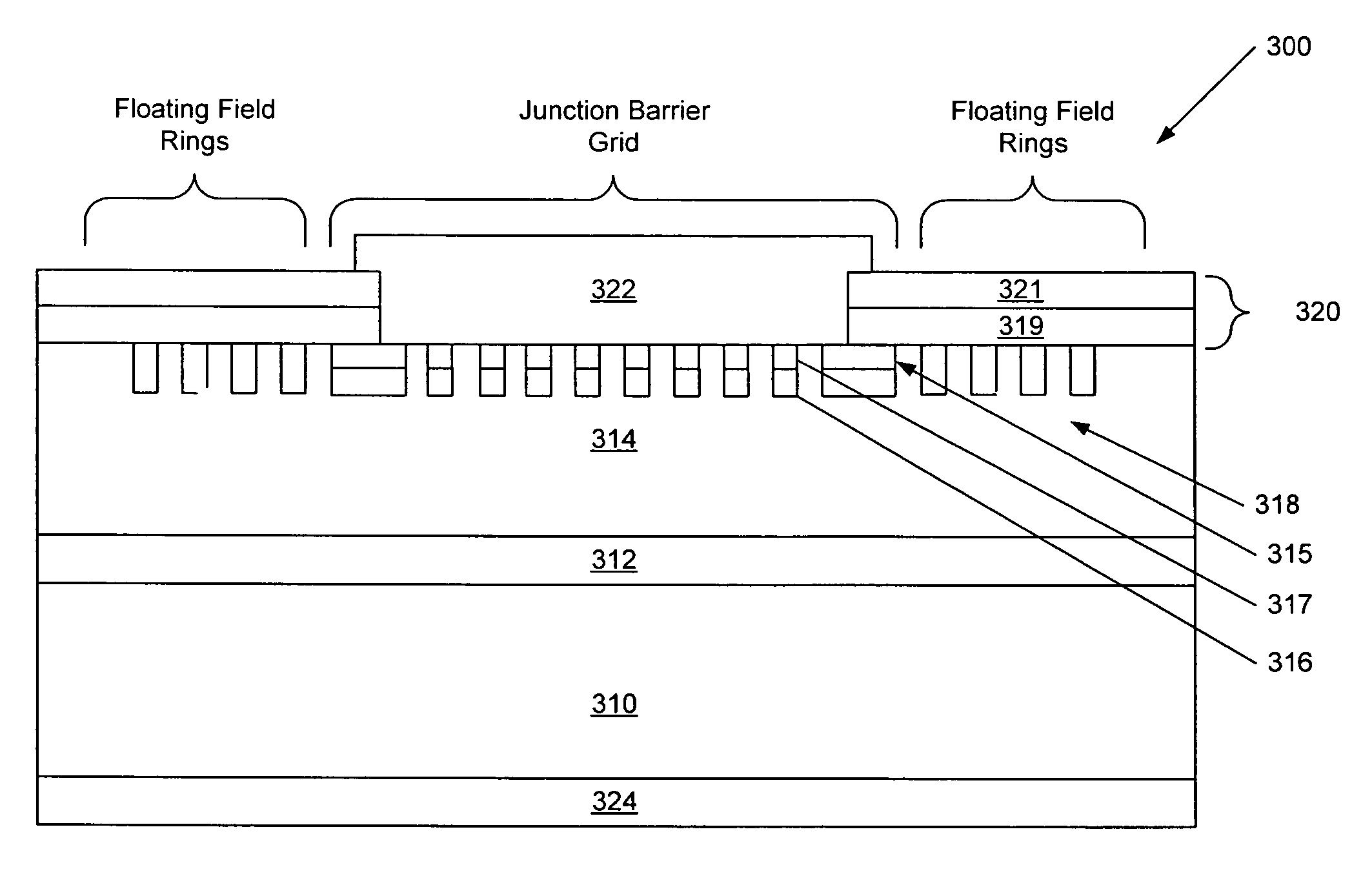
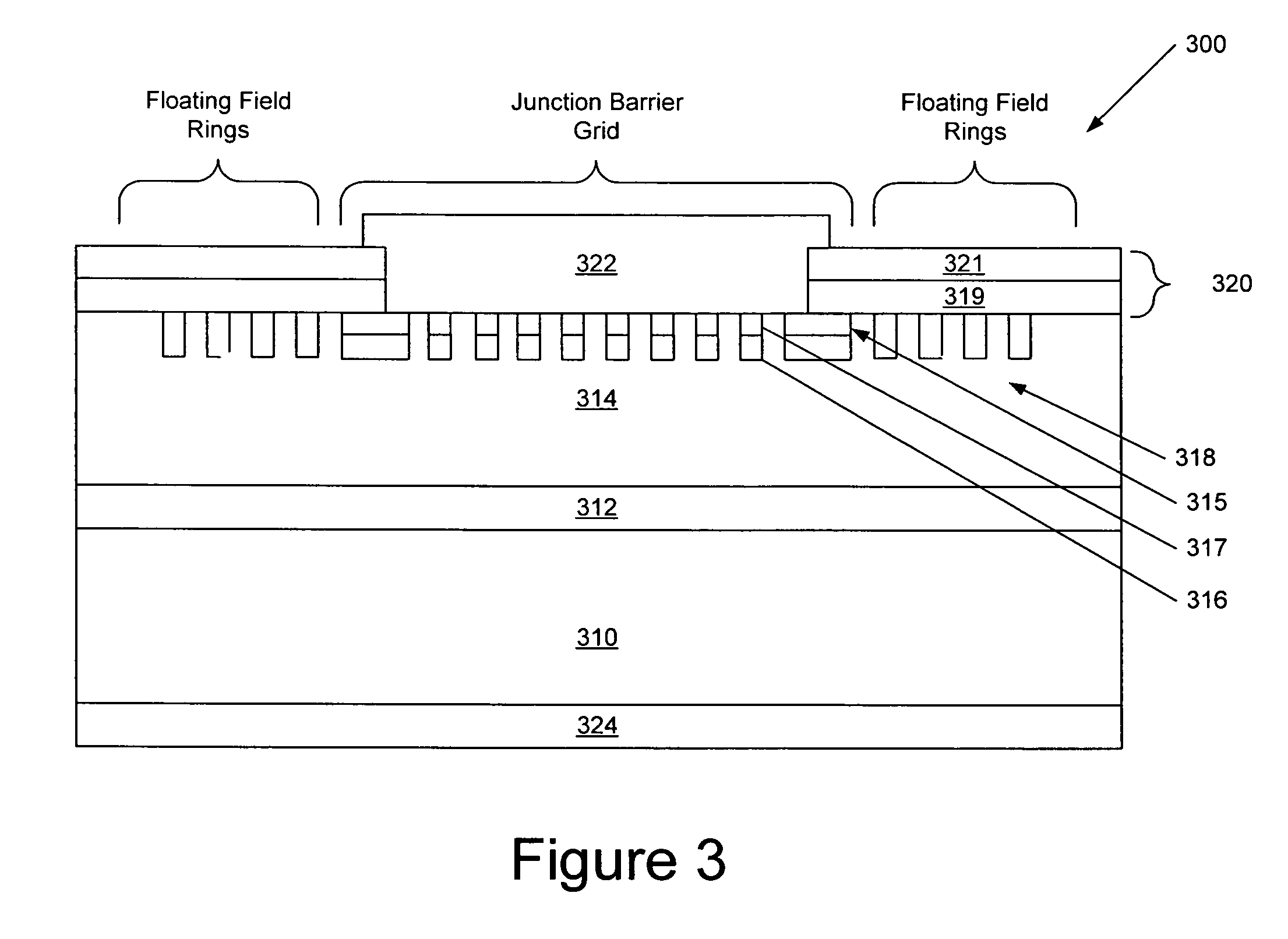
Integral structures that block the current conduction of the built-in PiN diode in a junction barrier Schottky (JBS) structure are provided. A Schottky diode may be incorporated in series with the PiN diode, where the Schottky diode is of opposite direction to that of the PiN diode. A series resistance or and insulating layer may be provided between the PiN diode and a Schottky contact. Silicon carbide Schottky diodes and methods of fabricating silicon carbide Schottky diodes that include a silicon carbide junction barrier region disposed within a drift region of the diode are also provided. The junction barrier region includes a first region of silicon carbide having a first doping concentration in the drift region of the diode and a second region of silicon carbide in the drift region and disposed between the first region of silicon carbide and a Schottky contact of the Schottky diode. The second region is in contact with the first region of silicon carbide and the Schottky contact. The second region of silicon carbide has a second doping concentration that is less than the first doping concentration.

Description

FIELD OF THE INVENTION [0001] The present invention relates to semiconductor devices and, more particularly, to diodes. BACKGROUND [0002] High voltage silicon carbide (SiC) Schottky diodes, which can handle voltages between, for example, about 600V and about 2.5 kV may handle as much as about 100 amps or more of current, depending on their active area. High voltage Schottky diodes have a number of important applications, particularly in the field of power conditioning, distribution and control. [0003] An important characteristic of a SiC Schottky diode in such applications is its switching speed. Silicon-based PIN devices typically exhibit relatively poor switching speeds. A silicon PIN diode may have a maximum switching speed of approximately 20 kHz, depending on its voltage rating. In contrast, silicon carbide-based Schottky devices are theoretically capable of much higher switching speeds, for example, in excess of about 100 times better than silicon. In addition, silicon carbide...

Claims


Application Information

Patent Timeline
Patent Type & Authority Applications(United States)
IPC IPC(8): H01L29/15
CPCH01L29/0615H01L29/0619H01L29/872H01L29/6606H01L29/1608H01L21/04
Inventor RYU, SEI-HYUNGAGARWAL, ANANT K.
Owner CREE INC
Learn More