Metal/semiconductor/metal (MSM) back-to-back Schottky diode

a back-to-back schottky diode technology, applied in semiconductor devices, digital storage, instruments, etc., can solve the problems of many conventional cross-point resistor memory arrays suffering from read disturbance problems

Active Publication Date: 2007-01-18
XENOGENIC DEV LLC
View PDF4 Cites 88 Cited by
  • Summary
  • Abstract
  • Description
  • Claims
  • Application Information

AI Technical Summary

Benefits of technology

[0015] Described herein is a back-to-back diode device that permits current flow in both forward and reverse directions under higher voltage (forward and reverse) bias conditions, but blocks current in under lower voltage bi

Problems solved by technology

Many conventional cross-point resistor memory arrays suffer from read disturbance problems, as electric current flows from a sel

Method used


Image

  • Metal/semiconductor/metal (MSM) back-to-back Schottky diode
  • Metal/semiconductor/metal (MSM) back-to-back Schottky diode
  • Metal/semiconductor/metal (MSM) back-to-back Schottky diode

Examples


Embodiment Construction

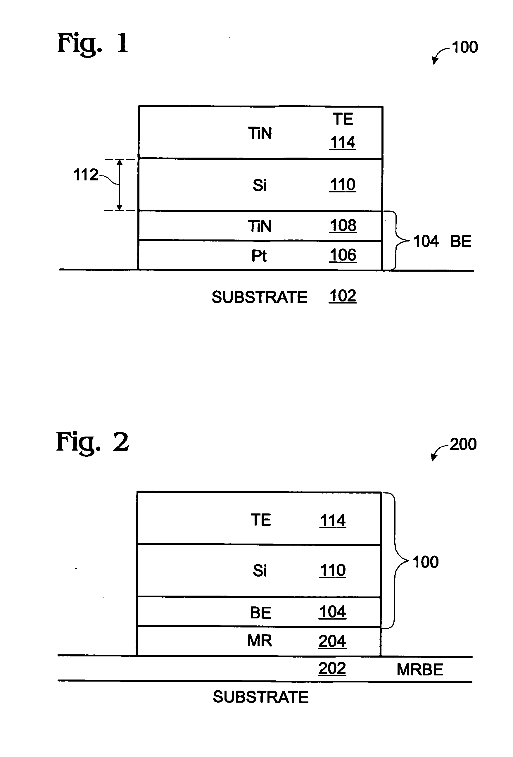
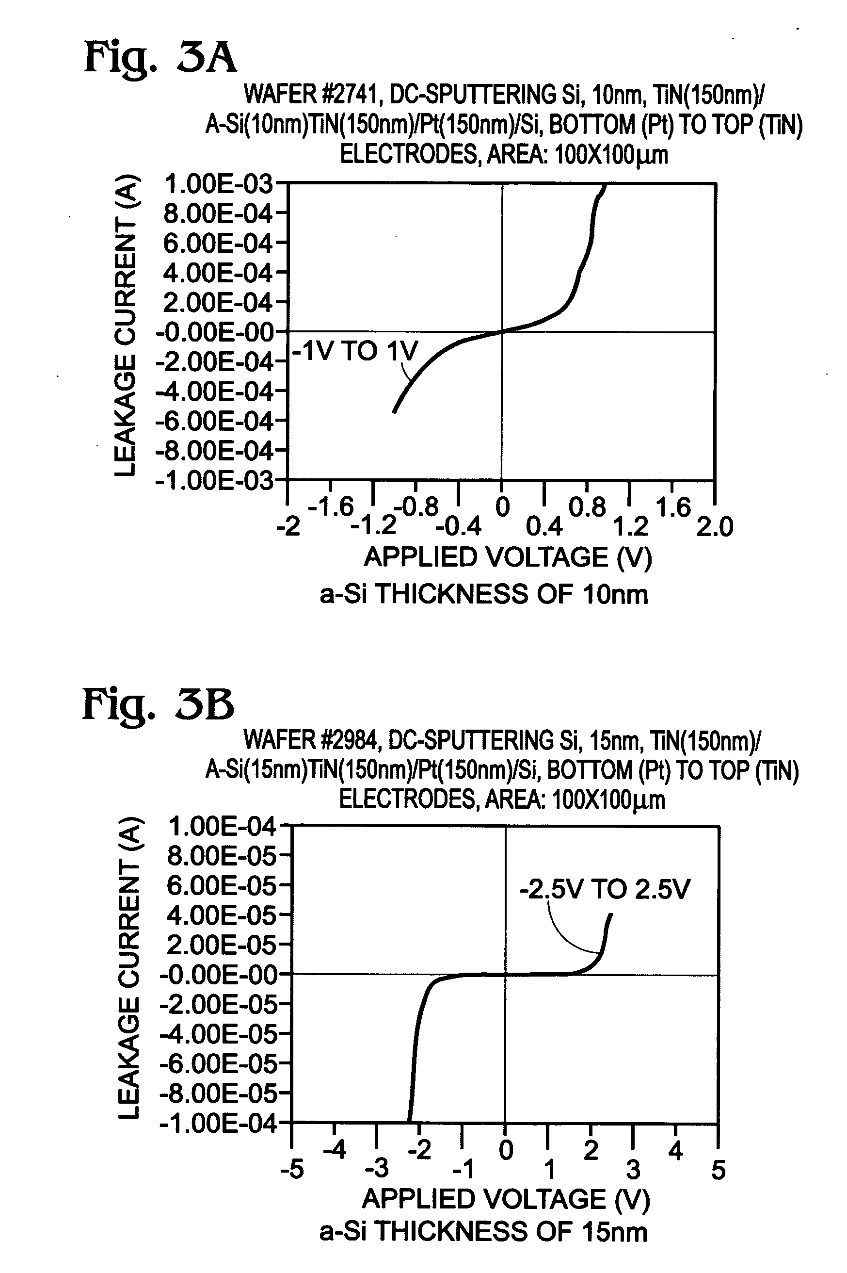
[0033]FIG. 1 is a partial cross-sectional view of a metal / semiconductor / metal (MSM) back-to-back Schottky diode fabricated from a silicon (Si) semiconductor. The MSM diode 100 comprises a Si substrate 102, and a bottom electrode (BE) 104 with a Pt layer 106 overlying the substrate 102, and a TiN layer 108 overlying the Pt layer 106. An amorphous Si (a-Si) semiconductor layer 110 overlies the bottom electrode 104. The a-Si semiconductor layer 110 has a thickness 112 in the range of 10 to 80 nanometers (nm). A TiN top electrode (TE) 114 overlies the a-Si semiconductor layer 110.

[0034] The a-Si semiconductor range of thickness may be considered unconventional, and even unexpected. As described in more detail below, the optimal device performance is dependent upon a thickness that must be balanced against considerations of threshold voltage, breakdown voltage, and on / off current ratio.

[0035] As described in more detail below, generally the MSM diode 100 has a threshold voltage in the ...


PUM


Abstract

A method is provided for forming a metal/semiconductor/metal (MSM) back-to-back Schottky diode from a silicon (Si) semiconductor. The method deposits a Si semiconductor layer between a bottom electrode and a top electrode, and forms a MSM diode having a threshold voltage, breakdown voltage, and on/off current ratio. The method is able to modify the threshold voltage, breakdown voltage, and on/off current ratio of the MSM diode in response to controlling the Si semiconductor layer thickness. Generally, both the threshold and breakdown voltage are increased in response to increasing the Si thickness. With respect to the on/off current ratio, there is an optimal thickness. The method is able to form an amorphous Si (a-Si) and polycrystalline Si (polySi) semiconductor layer using either chemical vapor deposition (CVD) or DC sputtering. The Si semiconductor can be doped with a Group V donor material, which decreases the threshold voltage and increases the breakdown voltage.

Description

RELATED APPLICATIONS [0001] This application is a Continuation-in-Part of a pending patent application entitled, MSM BINARY SWITCH MEMORY DEVICE, invented by Sheng Teng Hsu et al., Ser. No. 11 / 184,660, filed Jul. 18, 2005, Attorney Docket No. SLA0956. [0002] This application is a Continuation-in-Part of a pending patent application entitled, METAL / ZnOx / METAL CURRENT LIMITER, invented by Tingkai Li et al., Ser. No. 11 / 216,398, filed Aug. 31, 2005, Attorney Docket No. SLA0995. [0003] This application is a Continuation-in-Part of a pending patent application entitled, CROSSPOINT RESISTOR MEMORY DEVICE WITH BACK-TO-BACK SCHOTTKY DIODES, invented by Sheng Teng Hsu et al., Ser. No. 11 / 295,778, filed Dec. 7, 2005, Attorney Docket No. SLA0994. [0004] The above-mentioned applications are expressly incorporated herein by reference, and both claim priority under 35 U.S.C. §120.BACKGROUND OF THE INVENTION [0005] 1. Field of the Invention [0006] This invention generally relates to an integrated ...

Claims


Application Information

Patent Timeline
IPC IPC(8): H01L21/8242
CPCG11C13/0007G11C2213/31H01L27/101H01L29/66143H01L27/2409H01L45/04H01L45/1233H01L45/147H01L29/872H10B63/20H10N70/20H10N70/8836H10N70/826
Inventor LI, TINGKAIHSU, SHENG TENGEVANS, DAVID R.
Owner XENOGENIC DEV LLC
Why Eureka
Try Eureka