Method for producing a schottky diode in silicon carbide

a technology of silicon carbide and diodes, which is applied in the manufacture of semiconductor devices, semiconductor/solid-state devices, electric devices, etc., can solve the problems of limiting the possible reverse breakdown voltage, the simple structure illustrated in fig. 1 is not desirable either, and the formation of such a p-type guard ring is not simply implementable. , to achieve the effect of high breakdown voltage and simple implementation

Inactive Publication Date: 2005-05-24
STMICROELECTRONICS SRL
View PDF9 Cites 82 Cited by
  • Summary
  • Abstract
  • Description
  • Claims
  • Application Information

AI Technical Summary

Problems solved by technology

Indeed, the equipotential surfaces tend to curve up to rise to the surface at the periphery of the contact area, which results, especially in the equipotential surface curving areas, in very high field values, which limit the possible reverse breakdown voltage.
However, as previously indicated, the forming of such a P-type guard ring is not simply implementable by implantation / diffusion in a structure formed on a silicon carbide substrate.
In this case, the simple structure illustrated in FIG. 1 is not desirable either, for the same reasons as in the case of a silicon substrate.

Method used


Image

  • Method for producing a schottky diode in silicon carbide
  • Method for producing a schottky diode in silicon carbide
  • Method for producing a schottky diode in silicon carbide

Examples


Embodiment Construction

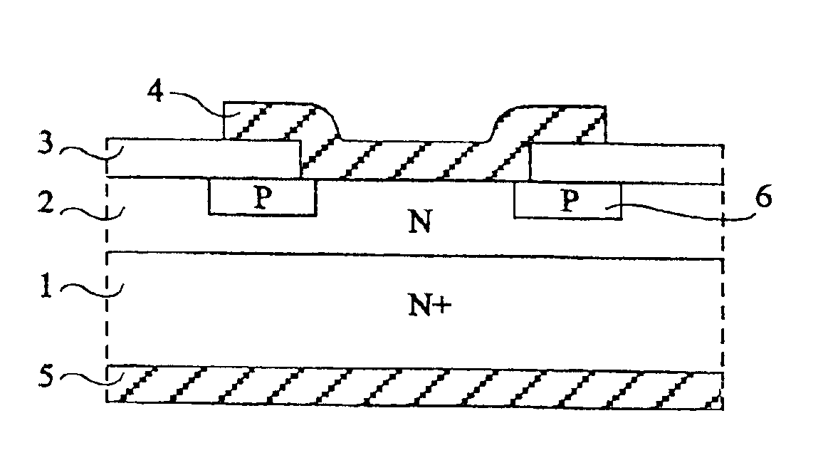
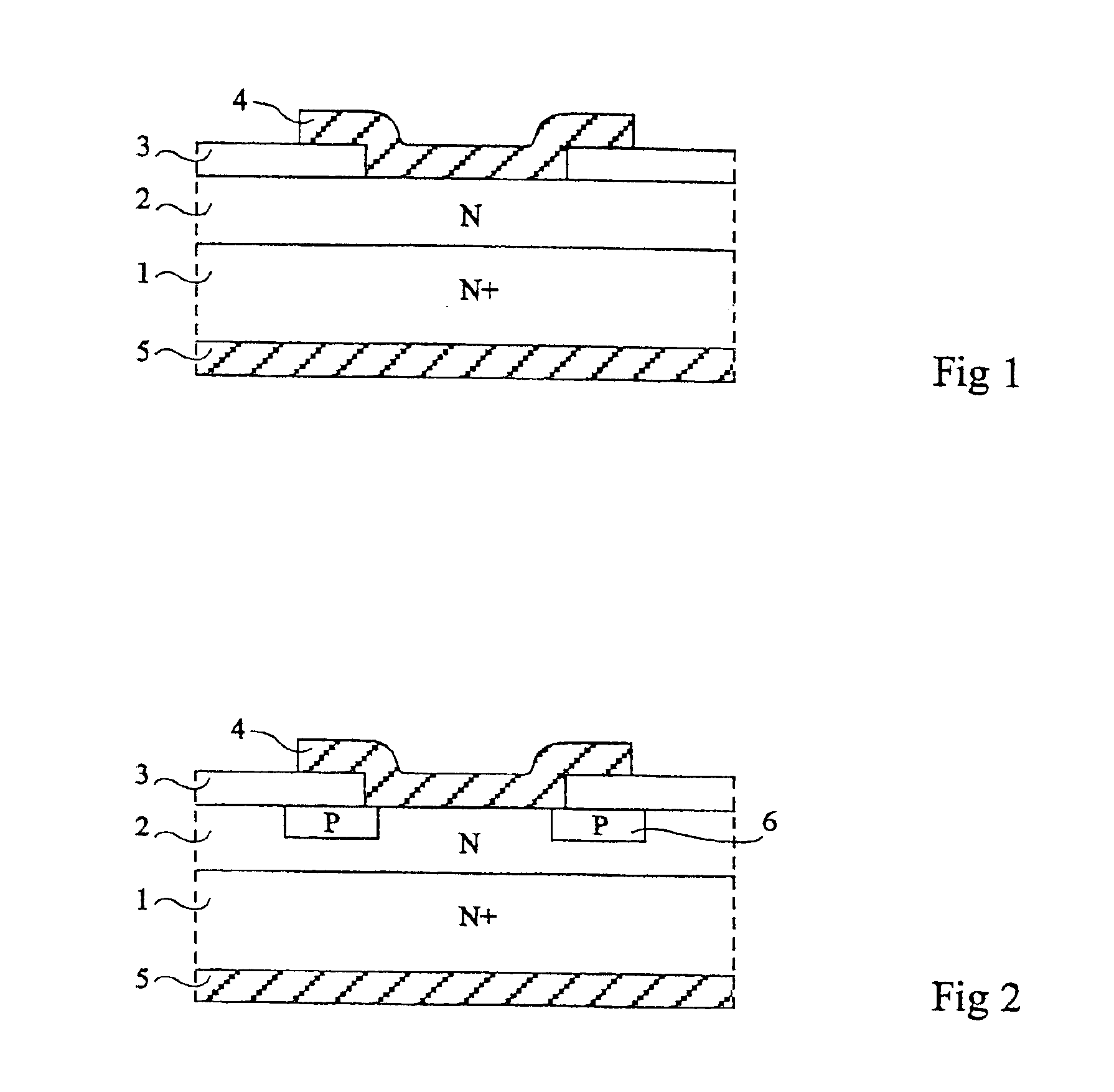
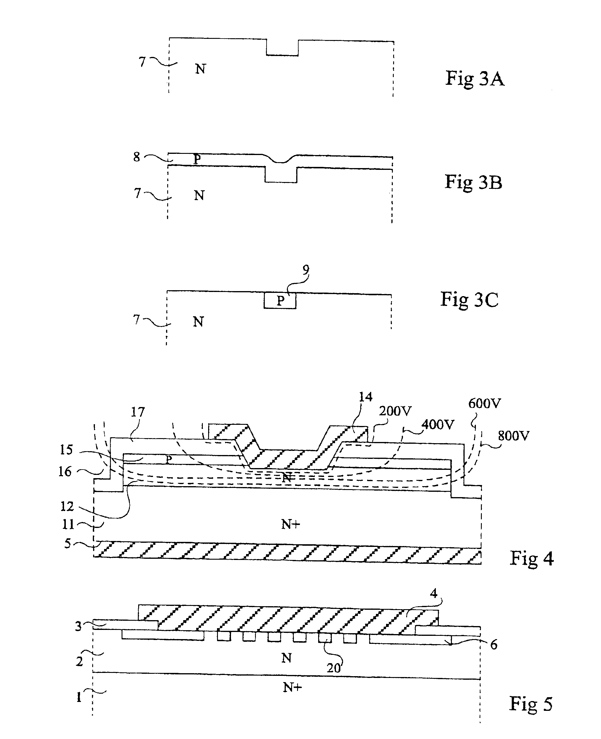
[0019]As usual in the field of semiconductor representation, in the various drawings, the various layers are not drawn to scale, either in their horizontal dimensions, or in their vertical dimensions.

[0020]As illustrated in FIGS. 3A to 3C, the present invention provides a succession of steps enabling formation of a doped area in a silicon carbide substrate without requiring use of very high temperatures.

[0021]At the step of FIG. 3A, a trench has been formed in a silicon carbide substrate 7. This trench has dimensions corresponding to those of the doped area which is desired to be formed and is formed by any adapted photolithographic etch method. Substrate 7 is a massive substrate or an epitaxial layer formed on a support.

[0022]At the step of FIG. 3B, a doped epitaxial layer 8 of the desired conductivity type, for example, of a type opposite to that of the substrate, has been formed. A P-type layer may for example be formed on an N-type substrate.

[0023]At the step of FIG. 3C, a plana...


PUM

PropertyMeasurementUnit
temperaturesaaaaaaaaaa
breakdown voltageaaaaaaaaaa

Abstract

The invention concerns a method for making a vertical Schottky diode on a highly doped N-type silicon carbide substrate (1), comprising steps which consist in forming an N-type lightly doped epitaxial layer (2); etching out a peripheral trench at the active zone of the diode; forming a type P doped epitaxial layer; carrying out a planarization process so that a ring (6) of the P type epitaxial layer remains in the trench; forming an insulating layer (3) on the outer periphery of the component, said insulating layer partly covering said ring; and depositing a metal (4) capable of forming a Schottky barrier with the N type epitaxial layer.

Description

BACKGROUND OF THE INVENTION[0001]The present invention relates to the forming of a Schottky diode in silicon carbide.[0002]1. Field of the Invention[0003]In the field of semiconductor components, the material which is currently mainly used is silicon. To withstand very high voltages, silicon carbide is a priori preferable since silicon carbide has a breakdown voltage per unit thickness approximately 10 times greater than silicon.[0004]However, in the present state of technologies, the processes currently used to form silicon-based components cannot be transposed to form silicon carbide (SiC)-based components. In particular, it is currently not possible in practice to perform implantations and diffusions of P-type dopants in N-type doped silicon carbide, noting that the P-type dopant currently used for silicon carbide is aluminum and that the N-type dopant is nitrogen. Indeed, an anneal for diffusion of an implantation of a P-type dopant would require temperatures on the order of 170...

Claims


Application Information

Patent Timeline
Patent Type & Authority Patents(United States)
IPC IPC(8): H01L21/02H01L21/04H01L29/66H01L29/872
CPCH01L21/0455H01L29/872H01L29/6606Y10S438/931H01L29/0619
Inventor COLLARD, EMMANUEL
Owner STMICROELECTRONICS SRL
Why Eureka
Try Eureka