Schottky Diodes Having Low-Voltage and High-Concentration Rings

a diode and high-concentration technology, applied in the field of integrated circuit devices, can solve the problems of unsatisfactory applications demanding high-performance schottky diodes, and achieve the effects of improving the breakdown voltage, reducing the leakage current, and increasing the on-current per unit area

Active Publication Date: 2009-12-03
TAIWAN SEMICON MFG CO LTD
View PDF10 Cites 83 Cited by
  • Summary
  • Abstract
  • Description
  • Claims
  • Application Information

AI Technical Summary

Benefits of technology

[0008]The advantageous features of the present invention include improved brea

Problems solved by technology

Further, the Ion/Ioff ratio, which represents the Schottky diode's ability to provide forward currents without causing significant leakage cur

Method used


Image

  • Schottky Diodes Having Low-Voltage and High-Concentration Rings
  • Schottky Diodes Having Low-Voltage and High-Concentration Rings
  • Schottky Diodes Having Low-Voltage and High-Concentration Rings

Examples


Embodiment Construction

[0018]The making and using of the presently preferred embodiments are discussed in detail below. It should be appreciated, however, that the present invention provides many applicable inventive concepts that can be embodied in a wide variety of specific contexts. The specific embodiments discussed are merely illustrative of specific ways to make and use the invention, and do not limit the scope of the invention.

[0019]A novel Schottky diode is provided. The variations of the preferred embodiments are then discussed. Throughout the various views and illustrative embodiments of the present invention, like reference numbers are used to designate like elements.

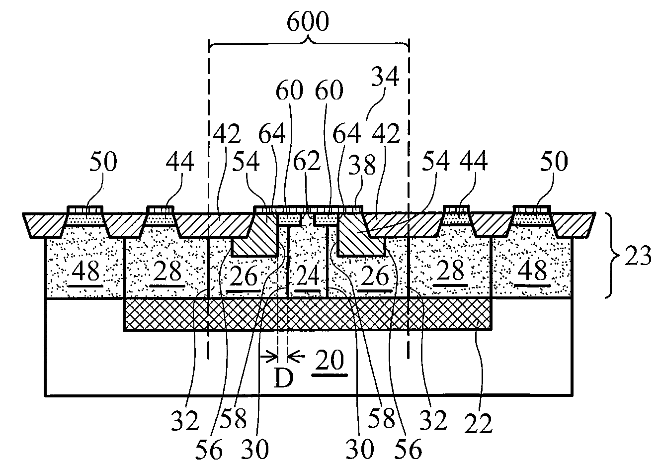
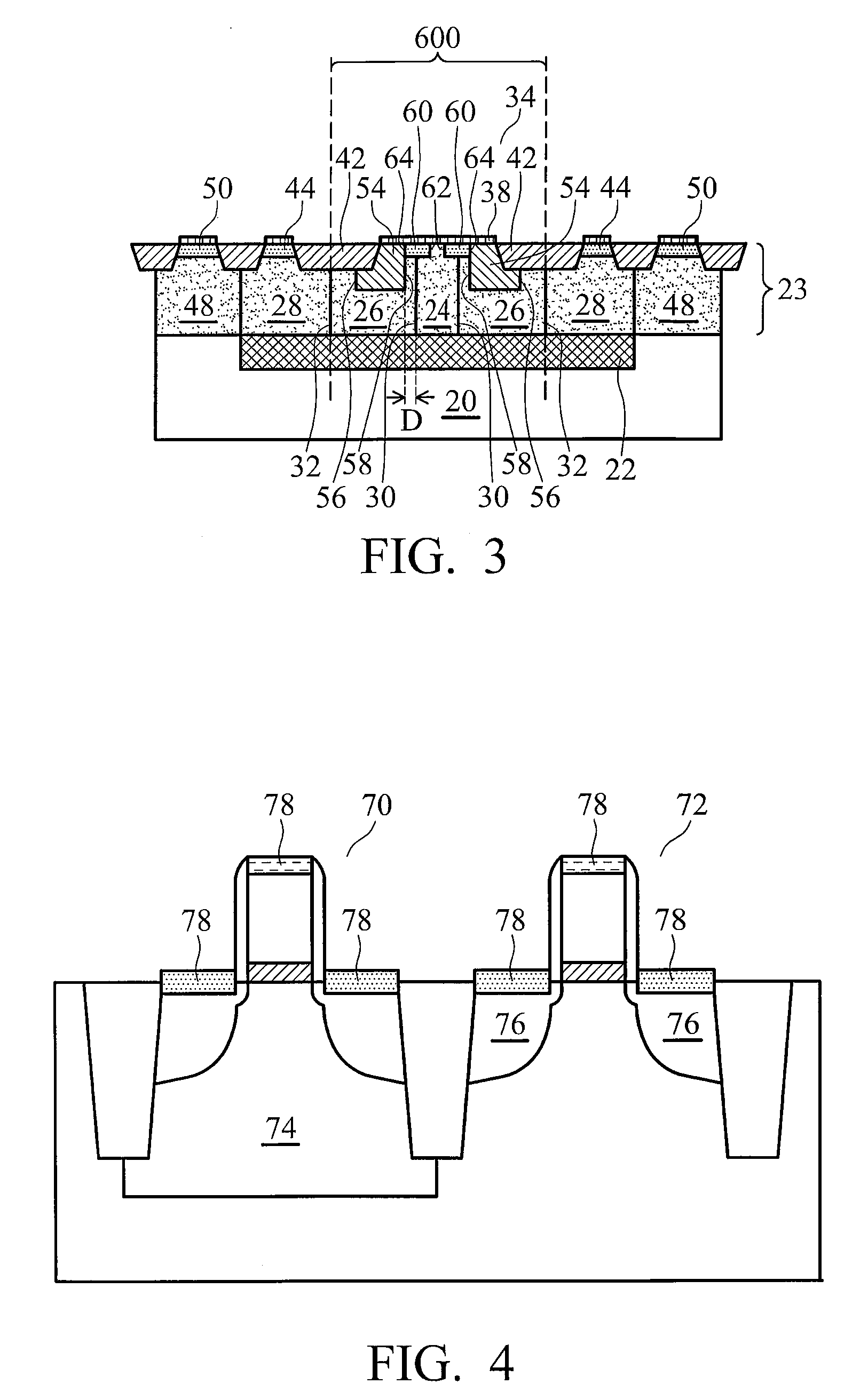
[0020]FIG. 3 illustrates a cross-sectional view of a Schottky diode embodiment of the present invention. Semiconductor substrate 20 is formed of a semiconductor material, for example, silicon or other group III, group IV, and / or group V elements. Preferably, semiconductor substrate 20 is of p-type. N-type buried layer (NBL) 22 is f...


PUM


Abstract

An integrated circuit structure includes a semiconductor substrate; a first well region of a first conductivity type over the semiconductor substrate; a second well region of a second conductivity type opposite the first conductivity type encircling the first well region; and a metal-containing layer over and adjoining the first well region and extending over at least an inner portion of the second well region. The metal-containing layer and the first well region form a Schottky barrier. The integrated circuit structure further includes an isolation region encircling the metal-containing layer; and a third well region of the second conductivity type encircling at least a central portion of the first well region. The third well region has a higher impurity concentration than the second well region, and includes a top surface adjoining the metal-containing layer, and a bottom surface higher than bottom surfaces of the first and the second well regions.

Description

TECHNICAL FIELD[0001]This invention relates generally to integrated circuit devices, and more particularly to Schottky diodes with improved on-currents and reduced leakage currents, and methods for forming the same.BACKGROUND[0002]Schottky diodes are commonly used in applications requiring fast switching, for example, in power circuits. Also, while standard silicon diodes have a forward voltage drop of about 0.6 volts, Schottky diode's voltage drop at forward biases of around 1 mA may be in the range of 0.15 V to 0.45 V, making it useful in voltage-clamping applications and in applications for preventing transistor saturation. Schottky diode's higher current densities further distinguish it from other diodes.[0003]FIG. 1 illustrates a cross-sectional view of a conventional Schottky diode 100, which is formed on p-type substrate 102. High-voltage p-well 104 is formed as a ring encircling high-voltage n-well 106. Shallow trench isolation ring 108 also encircles high-voltage n-well 106...

Claims


Application Information

Patent Timeline
IPC IPC(8): H01L27/06
CPCH01L29/872H01L27/0629H01L29/0619H01L29/0649
Inventor TANG, CHIEN-SHAOHO, DAH-CHUENJONG, YU-CHANGWANG, ZHE-YICHANG, YUH-HWAYADAV, YOGENDRA
Owner TAIWAN SEMICON MFG CO LTD
Why Eureka
Try Eureka